Skip to main content
Mobile menu
Discover
Develop
Agile
Resources & Support
Free Altium 365 Tools
Gerber Compare
Online PCB Viewer
Resources & Support
Learning Hub
Support Center
Documentation
Webinars
Altium Community
Forum
Bug Crunch
Ideas
Education
Student Lab
Educator Center
Altium Education Curriculum
Search Open
Search
Search Close
Sign In
Main menu
Home
PCB Design
Collaboration
Component Creation
Data Management
Design Outputs
ECAD/MCAD
HDI Design
High Speed Design
Multi-Board
PCB Layout
PCB Routing
PCB Supply Chain
Power Integrity
RF Design
Rigid Flex
Schematic Capture
Signal Integrity
Simulation
Software
Develop
Discover
Agile
Altium 365
Altium Designer
Education
Programs
Altium Academy
Engineering News
Guide Books
Newsletters
Podcasts
Projects
Training Courses
Webinars
Whitepapers
IoT Medical Product and Application Design: Challenges and Considerations
Ideally, any technology is going to drastically affect people and the ability of people to accomplish whatever tasks they need. Yet, when new technology is entering the medical domain, the stakes are always a bit higher: one has to be cognizant that any faults, errors, or malfunctions are going to immediately affect someone’s health. Granted, not every medical device is going to be life-or-death, but they should still be considered carefully
Read Article
Constraint Driven Design versus Rules Driven Design in a Unified Environment
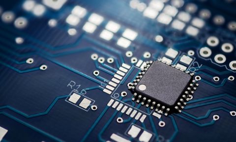
One of the most important productivity tools for PCB designers is a robust design rules checking (DRC) system or a constraints checking system. DRCs and constraints help ensure a PCB layout can comply with DFM requirements, signal integrity requirements, and custom place and route requirements that are specific to your product. Different programs display design rule definitions in different ways, design rules are defined in different interfaces
Read Article
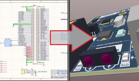
How to Create a PCB Layout from a Schematic in Altium Designer
You’ve done your usual excellent job of putting together the PCB schematic. The circuitry is defined and you are ready to go to PCB layout. But this time it’s a little different. Maybe your regular layout resources aren’t available, or perhaps you want to try to do your first layout yourself. Whatever the reason, you are ready to start working on the board side of PCB design, but you’re not sure how to create it from a PCB schematic in Altium
Read Article
PCB Design Software: Creating a Bill of Material using Altium Designer
You’ve done it, your printed circuit board is finished and ready for PCB assembly. The schematic is finalized, the layout is checked and approved and you are ready to get this thing built. To do that though, you need to create a bill of materials. Fortunately, we are long past the days where these documents were created by hand. Every CAD system out there will automatically create a bill of materials through some library or other process. But
Read Article
What's New In Altium Designer 18 Webinar Recap June 19
Altium Designer
®
Webinar: June 19th In case you missed our Altium 18 live webinar, no worries. You can catch up here with the video recording and presentation slides. If you’re not a fan of videos I’ll try my best to summarize in the webinar notes bellow. Most of the key takeaways will be the same as the may webinar but do take a look at the questions as they’ll be different. For future webinars if there’s something you’d like to see add it to
Read Article
PCB Routing Guidelines for DDR4 Memory Devices and Impedance
Follow these DDR4 routing and PCB layout guidelines to ensure signal integrity and correct timing for high speed DDR buses.
Read Article
Role of Embedded Capacitors in Circuit Board Design
Embedded SMD components like an embedded capacitor provide new levels of density that are beneficial in many systems. However, there are PCB manufacturing challenges.
Read Article
Commodore 128 Principal Engineer, Bil Herd on Best Practices for Learning a New CAD Tool
Curious about the early days of Early Home Computer Design? Former Commodore 128 Principal Engineer, Bil Herd shares stories from his illustrious career and Best Practices for Learning a New CAD Tool.
Read Article
Five First Pass Perils in PCB Prototyping Runs
The first pass prototyping run for a new design is where its functionality really gets put to the test. The functionality of your PCB depends on the quality of the design you create in your CAD tools, but sometimes the prototype just doesn't function as intended. There are many possible reasons for this, which could be related to your design choices, the capabilities of your manufacturer, or both. Founders without hardware experience might
Read Article
Annular Rings for PCB and Nonfunctional Pads: Should You Use ‘em or Lose ‘em?
Annular rings placed as non-functional pads in a PCB can affect via strength and signal integrity. Learn when to remove or keep them in this article.
Read Article
Pagination
First page
« First
Previous page
‹ Previous
…
Page
279
Page
280
Page
281
Page
282
Current page
283
Page
284
Page
285
Page
286
Page
287
…
Page
290
Page
300
Page
310
Page
320
Page
330
Page
340
Page
350
Page
360
Page
370
Page
380
Next page
Next ›
Last page
Last »
Subscribe to