Skip to main content
Mobile menu
Discover
Develop
Agile
Resources & Support
Free Altium 365 Tools
Gerber Compare
Online PCB Viewer
Resources & Support
Learning Hub
Support Center
Documentation
Webinars
Altium Community
Forum
Bug Crunch
Ideas
Education
Student Lab
Educator Center
Altium Education Curriculum
Search Open
Search
Search Close
Sign In
Main menu
Home
PCB Design
Collaboration
Component Creation
Data Management
Design Outputs
ECAD/MCAD
HDI Design
High Speed Design
Multi-Board
PCB Layout
PCB Routing
PCB Supply Chain
Power Integrity
RF Design
Rigid Flex
Schematic Capture
Signal Integrity
Simulation
Software
Develop
Discover
Agile
Altium 365
Altium Designer
Education
Programs
Altium Academy
Engineering News
Guide Books
Newsletters
Podcasts
Projects
Training Courses
Webinars
Whitepapers
PCB Design BOM Planning: A Balancing Act
The balancing act of knowing how much or little info is needed when designing your BOM is often convoluted and muddied. If done incorrectly, you could be stuck in a communication loop with a confused manufacturer, frustrated engineer, or a designer. This will inevitably cost you money, time and effort that otherwise would have been avoided. In order to assist us, today we’ll assume that you’ve begun to wrap up the final stages of your design, and
Read Article
Isolated vs Non-Isolated Power Supplies: The Right Choice Without Fail
Learn the advantages and disadvantages of isolated vs non-isolated power supply design.
Read Article
High Currents and High Temperature: PCB Design Tips for Heat Management
I remember the first (and hopefully the only) time one of my circuits caught on fire. It started with the resistors and quickly spread to a nearby decoupling capacitor. Thankfully, the destruction was minor and most of the components were salvageable. Why did this happen you ask? No, this was not due to a short circuit. Very simply, I did not take into account the high current PCB layout. As electronics continue to be miniaturized, the thermal
Read Article
Universal Language: PCB Design to Minimize EMI in Communications Systems
Can you imagine what a world without lines would be like? At first, it seems wonderful to not have to wait around anymore, trusting that people will figure their business out. Disneyland, happiest place on Earth, receives about 44,000 people per day. Imagine a thousand people all rushing to get on the next available log flume. No longer just a tower of terror, but a whole theme park. When designing PCBs, your traces are the lines and each has a
Read Article
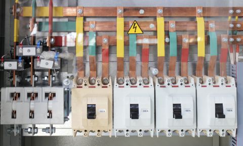
Be the Expert When it Comes to Designing Your Power Distribution PCB
Editorial credit: Paolo Bona / Shutterstock.com Around my house, we seem to undergo a transformation to obscure-sport experts every four years, and coincidentally it occurs at the same time that the Winter Olympics is taking place. Yes, I’m talking about the sport of curling. We have all become subject matter experts in the “button,” the “hammer,” the “house,” “sweeping,” and of course the “curl.” Rest assured, by next month we will have
Read Article
Design Medical Devices for Internet of Things and Your Hardware Capabilities
It seems like everyone I know has a smartwatch or fitness tracker. I gave mine to my mother when I felt like it was making me act weird (I sometimes put my laundry away one item at a time instead of using a laundry basket to get those extra step counts). There are days when I still covet graphs informing me of my status sleeping, walking, and eating. Fitness trackers barely scratch the surface of capabilities for medical IoT, though. Medical IoT
Read Article
How To Find Circuit Design Software Online: Search Parameters and Powerful Tools
Often, designers and companies will choose a certain PCB design tool based on factors other than what the tool is capable of doing for them. The chosen software may have a very low price tag associated with it, but does it do everything that you need it to do? This question goes much deeper as well. Not only does this software do what you want it to—but does it really excel? You may invest in an application that satisfies your needs today--but
Read Article
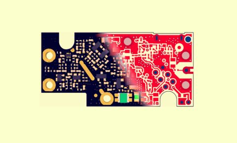
Increase Component Density in Multilayer PCB Design with Blind Vias
When I was still a novice circuit designer, my boards would be crammed with components. I later learned how to place components on both sides of the circuit board, freeing up some desperately needed real estate. If only there was a way to free up space by hiding traces below the surface of the circuit board... Newer devices are taking on smaller form factors, and the increasing demands for more capabilities will require that more components be
Read Article
PCB Floorplanning: The First Step to PCB Design Integrity
You’ve just received your first protoboards, and you are excited to put them into the product and fire them up. You love your design and you are ready to rock. The product goes into the EMI chamber, and it fails emissions. The product is noisy. You dive in with the test engineer to investigate. As you slowly unplug cables to isolate the noise, you find out your PCB is the cause. You think, no problem, I put filters on the board. You start
Read Article
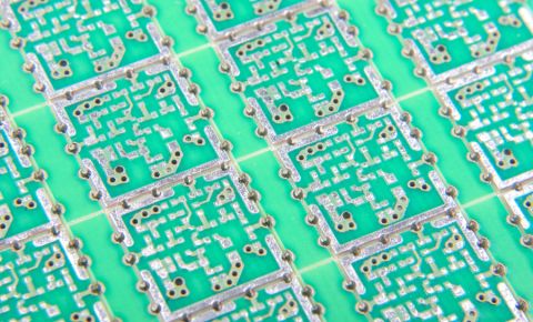
Optimizing PCB Panelization Can Reduce Costs and Increase Yield
Once you have finished designing your board, you are probably ready to move on to the manufacturing stage. Back in my research days as a grad student, our group always looked at ways to get the most out of our fabrication processes. But how do you maximize your device yield while still working within tooling and client constraints? The most efficient way to do this is to optimize your board arrangement during panelization. An analogue of
Read Article
Pagination
First page
« First
Previous page
‹ Previous
…
Page
298
Page
299
Page
300
Page
301
Current page
302
Page
303
Page
304
Page
305
Page
306
…
Page
310
Page
320
Page
330
Page
340
Page
350
Page
360
Page
370
Page
380
Page
390
Page
400
Next page
Next ›
Last page
Last »
Subscribe to