Tarun Amla on the Role of ITEQ, a Large Laminate Manufacturing Company in the PCB Industry

Tarun Amla is Executive Vice President and Chief Technology Officer of ITEQ. In this conversation, we dive into some of the mistakes product developers can make and the technological challenges they face. When it comes to laminates, Tarun is the industry’s noted go-to-guy, and is arguably the leading expert when it comes to determining the best suited laminate for targeted product applications. This article includes a description of ITEQ; the products and services it provides; its targeted market sectors; how it interacts with its customers; and common mistakes and material innovations going forward.
About ITEQ
ITEQ is a publicly-traded, leading manufacturer of cores and prepreg used in the fabrication of multilayer PCBs. The company was founded in 1997 and its headquarters is in Xinpu, Taiwan. In addition to its facilities in Taiwan, the company has fabrication facilities in Wuxi, Dong Guan, Guang Zhou, and Huang Jiang China, and its newest fabrication facility, commissioned in 2019, has just started production in Jiangxi.
ITEQ’s Xinpu location, its company headquarters, has a well-staffed, multidisciplinary product development team as well as an applications engineering group. This tech center includes a state-of-the-art analytical and failure analysis lab, a signal integrity and characterization lab, and a pilot scale facility for the scale-up of new products. In addition, the company provides a mass lamination service for those U.S. customers who don’t have the capability of doing inner layer processing. Along with its PCB laminates, ITEQ offers a line of flex products and has a fully-equipped R&D and Analytical Services Lab in Santa Clara, CA, USA, which includes state-of-the-art equipment for pilot manufacturing and signal integrity, thermal, mechanical, and physical testing.
About Tarun Amla
Tarun has more than 25 years experience in the laminate industry and has been awarded a number of ground-breaking patents for the various technologies he has developed. He has been running ITEQ’s R&D, in addition to other responsibilities, for the past three years, prior to which he held similar positions at other laminate manufacturers. He holds advanced degrees in Mechanical Engineering (Purdue) and Electrical Engineering (Stanford), in addition to an MBA (Northwestern – Kellogg).
The Target Markets
Tarun begins by giving some background on ITEQ. “We are the sixth-largest manufacturer in the world of laminate materials for the PCB industry and our revenue is more than $760 million per year. We are a fairly young company, and when we started, the automotive and consumer sector were the main product categories we targeted.”
“More than 95% of our business is in Asia. North America and Europe [however] are important for us, mainly because of the OEMs. For anything that is being built for OEMs in the U.S., most of it comes from Asia.”
Previously, the company’s mid-range Tg products accounted for most of its sales and they continue to represent a significant portion of its revenues. But now, the segment of the company that is experiencing the most growth is its low loss products targeted for networking and RF applications.
Tarun states, “Specifically, we go in high speed, low loss products such as servers, storage products, base stations (RRUs for 5G), switches and routers. This accounts for almost 40% of our revenue and we are probably the largest company in that space now. Right now, our sales are probably equally split between automotive and consumer electronics and networking products. But, if not this year, by next, low loss will be the highest-selling segment for us.”
In addition to the foregoing, ITEQ is looking to expand its footprint in the burgeoning 5G market space— particularly in terms of the antennas that will be required for those applications.
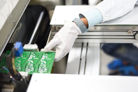
Figure 1 depicts the flow in a laminate manufacturing process.

Current Product Trends and How They Influence Material Characteristics
As noted in numerous other articles, end-use applications drive the specifics in terms of laminate performance capabilities. For ITEQ, the market focuses include:
- Automotive
- Networking
- Consumer electronics
- Mobility
“For the automotive sector, the emphasis is more on reliability—how many cycles can be achieved. This is because the applications, such as those found under the hood, are more thermally challenging. It’s about how many cycles you have to failure,” Tarun explains.
“Right now, the biggest drivers in the automotive market sector are electric vehicles. People want to charge their vehicles rapidly. This means you are putting a tremendous amount of voltage and current through the electronics. So the emphasis is on high voltage, high temperature, and low CTE (Coefficient of Thermal Expansion) materials for those applications. There’s also an emphasis on what they are calling high CAF reliability. This is about more breakdown resistance under high voltages.”
NOTE: CAF (Conductive Anodic Filament Failure) is the growth or electro-migration of copper that can occur in a PCB. It’s typically manifested between two oppositely biased copper conductors. The resulting failure can be manifested in four ways:
- Through hole to through hole (the most common failure mode)
- Line to line
- Through hole to line
- Layer to layer

Examples of CAF failures include intermittent electrical shorts, current leakage or breakdown of the dielectric between the conductors in a PCB.
For the high-speed networking area, Tarun notes, “56 Gbps has become the standard and now there is 112 Gbps. This is where PAM4 comes into play. I have even heard of 224 Gbps which means you would have a Nyquist frequency of 56 GHz. This is what the industry is looking for and that is the main challenge. The question becomes how do you make products with this kind of speed with the current technology?”
He continues, “For the HDI and mobility applications, the biggest concerns are dimensional stability and cost. For HDI, it’s about how thin you can go as well as the loss. Cost is also a concern but that is common across all applications.”
And, as has been noted in a variety of papers as well as industry conferences, copper is a major factor in today’s environment. Tarun explains, “When you have low loss products, almost 80% of that loss is dictated by the copper.”
On the high frequency side of the spectrum, everything is being driven by 5G. He states, “Right now, there is a little bit of a waiting period because some of the ICs are not yet available. We’re really going to millimeter wave. That’s the trend and everyone is gearing up for that. Right now, for 5G, most of the deployment has been below 6 GHz which is sort of like an extension of 4G LTE. Whether you classify it as 5G or millimeter wave, the focus will be on ultralow loss, high thermal conductivity materials. And, of course, the desire will be to have very stable electrical and thermal properties. The service conditions will be very stringent. We’re talking about 130˚C continuously for many years.”
“With 5G, we have not really seen much in terms of how smartphones will evolve. They are most likely going to have four to six beam forming units in them. In order to form these units, they will have to be packaged with flex materials. That’s a major trend and a major challenge.”
Customer Interaction
To a certain extent, the information that ITEQ needs from its customers to determine which laminate will be the best for them is dependent on the targeted market sector.
As Tarun describes, “In the high speed arena, we need to know what a customer’s overall loss budget is, as well as the geometries and impedances they are working with. We also need to know what the loss factors are and what the reliability requirements are; such as cycles to failure, CAF requirements, plated through-hole reliability and, as noted previously, dimensional stability. We also need to know what the service conditions will be. If this information is not explicitly provided, we have to ask these questions.”
“The first thing we do is to run simulations. Then, we build test vehicles. The major OEMs will have test vehicles that they go for and will provide us with the design, but, in most cases, the onus is on us to simulate and use an industry standard test vehicle for the customer. They will indicate that they have a preferred supplier. The first thing we do is to provide the simulation. Then, assuming the cost and other parameters are in line, we build the test vehicle with that preferred supplier. Next, the desired measurements are extracted from the test vehicle. In most instances, this is done through third-party laboratories. The customers like our information and they want to trust what we tell them, but they also want to independently verify it. We understand that this is part of the process.”
Common Mistakes Product Developers Make
The knowledge base of the product developers, as well as their experience in building real-world products, plays a big role in terms of their ability to select the right laminate for their particular product.
Tarun notes, “Most of the major OEMs are well-staffed. They will have a PCB guy on their staff. In some instances, they will even have a person who has some laminate experience. For high-speed implementations, they know what they are looking for and they have a clear understanding of what is involved. And, they will design the stackup for signal integrity. But they won’t look at it with respect to cost and reliability.” He adds, “They will typically not put an emphasis on what kinds of challenges might be imposed on the fabricator and on how long the product has to survive. In this regard, they tend to have a one-dimensional approach. That’s why we put a product through its paces by sending it through a test vehicle process.” Tarun continues, “There are definitely gaps with newer players and smaller players. If you go to any of the forums out there, you understand that people are not well versed. The new guys and the small guys don’t have that much information. They struggle and they go to these forums and they try to find information. They don’t want to engage [with the laminate suppliers] because they don’t want to come off as unknowing. I think if they were to talk to a laminate supplier they would get a lot of things cleared up. That’s where the education process comes into play.”
“Probably the first tendency, for people who fall into these gap categories, is to go to the website and try to find the information they need there. But, sometimes, when they go to the website, they will pick a laminate based on a single data point such as the Dk or Df at a low frequency for something that they will be using at a much higher speed. They don’t realize that the electrical properties change with thickness and construction. Or, again, on the stackup, they don’t understand the resin volumes and what’s needed to flow and fill and encapsulate the circuitry. Maybe there won’t be enough or too much prepreg or perhaps they are using too much heavy copper.”
Challenges Going Forward and New Materials to Address Them
As noted in previous articles, there are a number of challenges facing the industry as we go up the speed curve and move to ever decreasing device geometries. In addition to these factors, Tarun notes, “We have reached the stage where copper is dominating loss. One of the misconceptions in the industry comes from simulation tools that understate copper loss. As a result, people tend to think the dielectric losses are higher than they really are. In any case, the emphasis is on lower and lower loss. Every five to ten percent you can squeeze out of loss is going to be important.”
“The key issue is what is going to happen on the copper front because we are pretty much at the end of the road in terms of how much lower we can go with the copper roughness or oxide roughness profile. But, this issue is not in our domain. It resides with the oxide and copper suppliers.”
He continues, “One of the major breakthroughs that we have is a new skew-free product that is ultra, ultra-low loss. It’s been validated and most of the OEMs are anxious to get their hands on it. In this product, we have done away with the glass. If you don’t have woven glass, you aren’t going to see skew.”
Note: As stated in previous articles, some advances have been made relative to skew as a result of the mechanical spreading of the glass weave. However, there is still no industry consensus on the spreading process itself so skew continues to remain a problem.
Tarun notes, “A lot of people are trying to get to next-generation lower Dk glass. This is still woven glass and it is still going to have skew problems. The reason that people want thinner copper lines is that they have to rotate the PCB to eat up a lot of the real estate. If you have a skew-free laminate, you don’t have to do that. With this laminate, you can get thicker lines and still be able to have a very high density board that still has lower loss. That’s the position we are taking with this laminate. First, we are addressing the immediate issue of loss. Then, as product developers see the benefits of no skew, they will also see the benefits of being able to use the board real estate better because there is no need for serpentine traces. This product is the one that we would position for 112 Gbps applications at 28 GHz Nyquist (as noted earlier).”
“We are also trying to get to a stage where we can make products that have loss equal to or lower than PTFE (polytetrafluorethylene). These products would be more for RF (mainly 5G and mmWave) applications. In these instances, the boards are thicker and the lines are wider so copper is not as significant of a problem.”
“In addition to ultra low loss products for 5G applications, we are looking at flexible laminates for other smartphone and antenna applications.”

At the time of the writing of this article, it’s apparent that the COVID-19 pandemic can potentially have wide-ranging impacts on all types of business across a broad spectrum of different industries. The extent and the length of time that the overall high-tech industry, as well as a multitude of other businesses and technologies, will be impacted is still unknown.
Specifically, the laminate industry has been impacted because 80% of the industry is centered in China. Tarun explains, “The incidence of new infections has gone down in China and manufacturing is back up. What we have been hearing is that everything that is new has been dropped and the focus is on getting the boards built that have already been put on order. One of the things that has happened is the OEMs are seeing the result of having jettisoned all of their ties to North American fabricators. There is a bit of a panic because there isn’t anyone in the States that can be geared up to build the boards. All of these plants in the U.S. have basically disappeared and there are no signs that they will ever return.”
He adds, “Long term, we really don’t know how this is going to affect us as an industry because it is something that is still evolving. So far, the impact has been businesses cancelling conferences and banning travel. But, at least, we have technologies available that allow us to effectively communicate.”
COVID-19 is not the first incident in which this industry has seen the impact of losing a sole-sourced supply chain item. In 2011, the tsunami that hit Japan following the earthquake destroyed the Nittobo glass factory. It was the sole source of the low Dk glass used in PCB laminates aimed at the low loss market, and there was nothing to replace it. At that time, and for some time afterwards, there were warnings across the industry against having too much of its supply chain based in any one global area. But, so far, it’s not clear that we have learned the lesson.
Summary
The laminate production and supply process is driven by the types of products being developed for specific targeted applications. For product developers, having a clear understanding of the various types of laminates and their performance characteristics is one of the first steps in creating a successful design.
Talk to an Altium expert today to learn more.


