


Anatomy of Latitude Part One: Pulse Width Modulation (PWM) as a Result of the Evolution of Linear Systems


Great Ideas and Smart Solutions
There are different techniques in the world of technology to achieve various goals, both final and intermediate. Some techniques are so successful that they are commonly used with high efficiency. Electronics is no exception. Great ideas and ingenious solutions are found and applied in this area probably more than in other engineering fields. The greatest example is the use of Pulse Width Modulation (PWM) signals (energy), which is applied in any modern electronic device whether it is an autopilot, smartphone, tablet, laptop, LED spotlight, or even an electronic toy, and helps to effectively and economically solve the following issues:
- Voltage or current transformation for power supply of individual circuits, nodes and units of an electronic device (supply voltage stabilization for circuits, current stabilization for LED-based lighting devices)
- Highly efficient amplification of the audio signal power range (audio power amplifier Class D with an efficiency close to 100%)
- Control of actuators such as hydraulic or pneumatic valves (drives of aerodynamic surfaces of wings, rudders of aircraft and rockets, automatic transmissions of cars, control units of internal combustion engines and turbines, industrial automation in the broadest sense)
- Converting a digital code to a specific proportional voltage or current value (an alternative to many DACs)
- Transfer of information (including execution commands) about the position of the operating device (e.g., control of UAV and robot steering gears)
This fact puts PWM at the top of the list for in-depth study and review in real and practical applications.
To apply PWM effectively, it is necessary to understand the engineering difficulties that engineers faced in the past, and the thoughts and ideas that subsequently were combined into effective, complete PWM power solutions.
Engineering Difficulties
As an example, there is a device that requires a stabilized supply voltage of 5V and consumes a current of 2A. We have a power supply with an output voltage from 10V to 36V. How can we use it to power our device? The first thought is to use a linear regulator in order to "dissipate" the extra input voltage over 5V. Therefore, let’s create and simulate a linear voltage regulator for our device and analyze its characteristics using Altium Designer - Mixed Simulation*.
Note: To eliminate the problem of finding components with special characteristics, a schematic will be created using the electronic components of the standard library Simulation Generic Components integrated into Altium Designer.
In the new project, we create the "Linear regulator" schematic based on the operational amplifier.
The schematic presented is largely idealized and consists only of components, which represent only the idea. The operational amplifier compares the reference voltage V2 Ref with the voltage on the R1 and applies the control action to the bipolar junction transistor Q1, which has the function of a regulating element. In our case, the schematic maintains the output voltage V(Load)=5V equal to the reference voltage V(Ref).
Note the value of R1. The simulator allows you to enter not only strict values but also mathematical representations and dependencies as a value. In our case, this is the formula of Ohm's Law: 5V/2A, i.e. 2.5 Ohm, and of course, instead of a fraction you can just write 2.5 and the result will be the same.
In order to display voltages in the schematic nodes, run the Operating Point calculation then select the display of the required physical quantities: Voltage, Power, Currents.
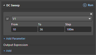
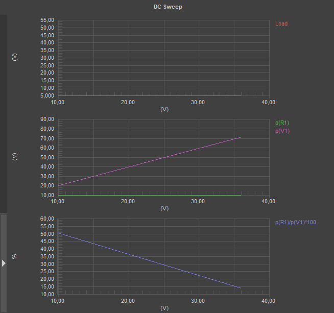
But the initial condition is the following: the source produces voltages in the range of 10-36V, so it is important for us to see how the schematic behaves in these conditions, i.e. we need to build the function V(Load)(V(V1)). This allows us to configure the following type of DC Sweep analysis.
-
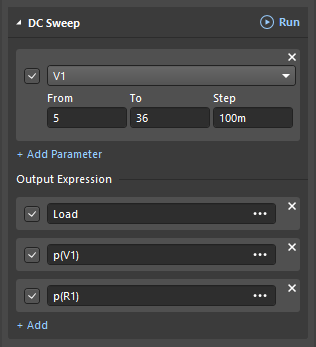
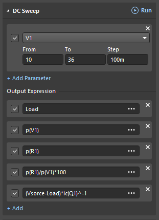
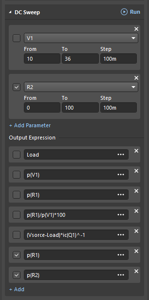
In DC Sweep, select the V1 parameter that we will change then specify its range of 10-36V with 0.1V step.
-
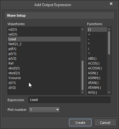
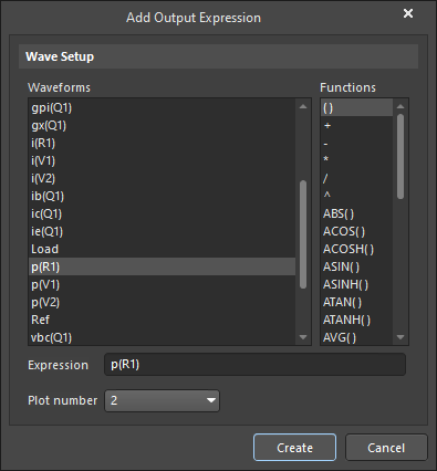
In the Add Output Expression dialog, specify/add (+Add) the value we want to see on Plot 1.
-
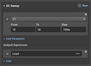
As a result, we have a function V(Load)(V(V1)) configured to display on the plot.
-
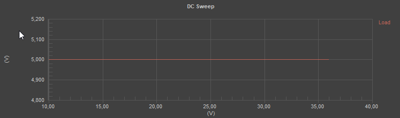
Run the calculation by clicking Run in the DC Sweep field; the Simulator immediately displays the plot.
-
Abscissa axis - input voltage V(V1)
-
Ordinate axis - load voltage V(Load) equal to 5 volt
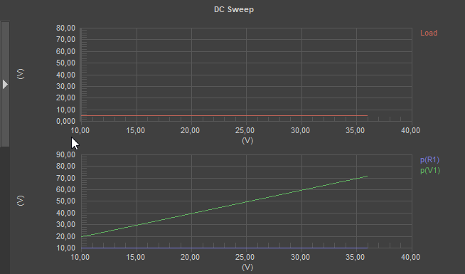
We can see that the schematic works correctly in the whole range of the input voltage.
Let’s evaluate the efficiency of this solution. We need to compare the total power of the schematic, which is equal to the output power of the source V1, with the effective power in the load R1. To do this, we add (+Add) to the Add Output Expression dialog in the DC Sweep new functions on the input voltage V(V1) on the required components, such as P(R1), (V(V1)), and P(V1)(V(V1)), and display them on Plot 2.
Run the DC Sweep then review the plots.
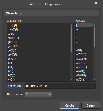
When the input voltage is 10V, the power in the load is half the power from the power supply, i.e. the schematic efficiency is 50%. When the voltage is 36V, you can also evaluate the value with a calculator. However, the Simulator can do it more clearly. It is necessary to add (+Add) to the Add Output Expression dialog in the same DC Sweep function to calculate the efficiency of the schematic.
Enter “P(R1) / P(V1) ) from V(V1) * 100as the Expression and place the result on Plot 3.
Run the DC Sweep then review the plots.
The result is disappointing. Plot 3 clearly shows how the supply voltage of the schematic increases and its efficiency decreases linearly from 50% to 14%. If we create such a schematic, the cost of the radiator will be several times higher than the total cost of the electronic part of this schematic, without considering the low efficiency of energy use. This scenario makes us search for solutions that will improve the efficiency of energy transformation.
Despite the negative result, we can see potentially promising results. In this situation, there is an increase in the efficiency of the schematic while the voltage drop was reduced to the regulating element. What does this mean?
“Over-the-horizon” Perspectives
Now, let's see the equivalent resistance of the regulating element from the input voltage. To do this, according to Ohm's Law, we divide the voltage drop across the regulating element by the current flowing through it as described below.
-
Rq1 = (Vsource - Load) / IcQ1 (since the base current of transistor Q1 is much smaller than the collector and emitter currents, we ignore it and assume that the collector and emitter currents are equal)
-
DC Sweep will help us. Let's add (+Add) this Expression to the Add Output Expression dialog.
Note: For convenience, we express the ratio 1/IcQ1 as (IcQ1)^-1, so the function is as follows: (Vsorce-Load)*ic(Q1)^-1:
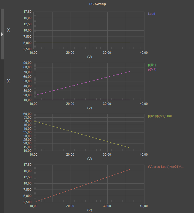
Let's take a look at the entire list of plots we have built.
Run the DC Sweep then review the plots.
The lower plot is the change of equivalent resistance Rq1 of transistor Q1. When the efficiency increases, the Rq1 decreases, i.e. the lower the resistance of the regulating element, the higher the efficiency. Let's study what will happen if the resistance of the regulating element becomes zero and check where and what kind of power will be generated. Let's replace transistor Q1 with resistor R2 and see how its resistance affects the power balance in the schematic (we are not interested in the voltage on the load R1).
In order to do this, we add a resistor to the schematic and hide the electronic components that are not used with the compilation mask.
8:35
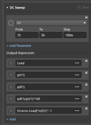
This time, we disable (not delete) previously calculated unnecessary dependencies in DC Sweep by unchecking the appropriate boxes.
Select R2 parameter in the DC Sweep (that we want to change) then we specify the range of 0-100 Ohm with 0,1 Ohm step and add (+Add) new features in the Add Output Expression dialog: P(R2) and P(R1) on R2.
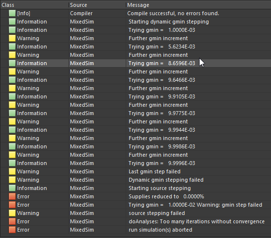
Run the DC Sweep. There will be many errors, which are displayed near the bottom of the Messages panel below the plots.
We did everything right, but there are some limitations when working with the Simulator, which you need to know in order to use the Simulator. The fact is that the Simulator is a mathematical machine that works in a "digital organism" that is limited in its ability to represent super small and super large numbers for which it sometimes (but not always!) fails. In our situation, the Simulator apparently divided something by zero during calculations. The Simulator does not like zeros and infinity of resistances and conductivities.
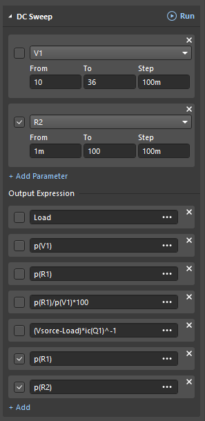
In this task, the Simulator failed at the zero value of resistance R2. This problem is easy to solve. Instead of 0 Ohm, we must enter a small, non-zero value, for example, 1 mOhm, that does not affect the quality of the result. The Simulator now handles this easily.
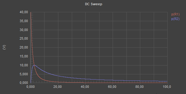
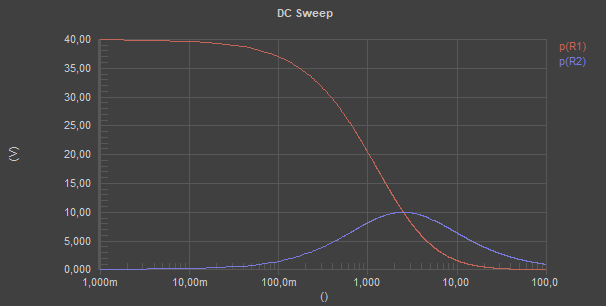
Run the DC Sweep and review the plots.
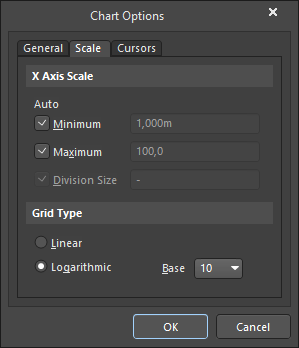
Let's look closely and we can see... But no! Perhaps it's wrong to gaze, too. The simulator is not only a mathematical machine but also a telescope and a microscope at the same time. It allows you to conveniently see both small and large in the same window by logarithmically distorting the display area, i.e. expanding the small and compressing the large. Open the Chart Options dialog by double-clicking on the horizontal abscissa axis of the plot.
Enable the Logarithmic option then click OK. The results are shown below.
The horizontal axis is divided into equal sections and their limits differ not by 10 ohms (as in the previous plot), but by a factor of 10. Now you can see on the same scale what is going on in the ranges and 0.1-1 Ohm, 1-10 Ohm, and 10-100 Ohm.
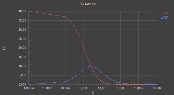
Looking at the result, it feels that the possibilities of this representation on the right have not yet been fully exhausted, so let's increase the upper range in DC Sweep for the parameter R2 by a factor of 100, i.e. up to 10 kOhm.
To evaluate the difference in interpretation, independently evaluate the informativeness of the plots in linear and logarithmic scales by enabling the appropriate options in the Chart Options dialog. Keep in mind, nothing is what it seems, and what you see in both linear and logarithmic scales is the same thing. That's the magic of logarithm.
Let's return to the analysis of the plots. The red plot is the power transferred to the load - R1 and the blue plot is the power dissipated to the regulated element - R2. As you can see, if you change the resistance of the controlled element intermittently (i.e. as fast as possible) from 0 to infinity and back, you can supply energy from the source to the load in portions without losing energy on the controlled element! This mode of the regulated element is known as a key mode, and the regulated element functioning in this mode is often named the Key. The absence of energy loss on the Key, at the extremes of its resistance, is very interesting for the application. The key mode is the basis of PWM energy operation and allows you to solve the problem of its conversion with high efficiency.
It's time to look inside the PWM and to understand its anatomy in the second part of our story: "Thread with a Needle” in the context of energy.
Related Resources
Table of Contents
Design to Release, Without the Friction
- Keep reviews tied to the right version
- Reduce handoff confusion and rework
- Spot sourcing and release risk earlier
- Work solo, share when needed
Get Started
Thank you, you are now subscribed to updates.

