The Altium PCB Auto Router: The Best PCB Automated Routing Tool

Routing traces on your printed circuit board is that critical step during layout that creates the connectivity and functionality your board needs. It can also be time-consuming if your design autoroute software doesn’t contain the right routing tools. Your PCB design software should include high-precision routing tools that are designed to automate many portions of the routing process. Advanced PCBs require the best PCB auto-router, and your automated routing tools should help you design PCBs with maximum efficiency.
Altium’s PCB Autorouter tool provides fully automated and semi-automated routing for any device and is built on the most advanced routing algorithms. The auto-router will quickly apply routing to your PCB and connect even the most complicated boards. ActiveRoute for Altium Designers is an interactive routing feature that allows the user to take control over automated routing. You can reduce your design time and create higher-quality products with the Autorouter tool in Altium Designer. Read on to learn more about interactive and automatic routing.
ALTIUM DESIGNER
A PCB design software package with the best PCB editor and automated routing tools.
Routing is perhaps the most tedious task in the PCB design process. Experienced designers enjoy the challenge as they get to apply their creative puzzle-solving talents to create a work of art. Designers who are new to the task and those who would rather focus on other aspects of design, struggle in execution.
Thankfully, there are plenty of PCB design tools that can cut down on design time. The Altium auto router helps PCB designers with the difficult-to-master process of dense trace routing on a PCB. It seems like a rather simple task: connect a copper line from point A to point B with your schematic capture output as a guide. Altium Designer’s PCB autoroute tools help speed up the process of trace routing in a complex circuit board. Here’s how the different routing features in Altium Designer work and how they can help you create the best new PCBs.
It All Starts With a Routing Strategy
In a real PCB, you’ll be connecting tens or hundreds of these lines between components, and fitting all of these traces on your board is a difficult task. If you want to use an autoroute PCB tool, you need to incorporate it into a larger routing strategy. You may need to route different functional blocks through different layers, or you may need to route layers sequentially. Whatever path you choose to take, you can configure these settings in the Altium auto-router.
Unlike older auto router PCB tools, which operated in their own environment and required their own setup, the Altium auto router is part of the rules-driven design environment in Altium Designer. Instead of spending valuable time with complex router setups and data transfers, you simply configure the auto-router PCB tool and it will route traces that satisfy your PCB design rules and constraints.
Altium Auto Router Results
The figures below show a PCB auto router comparison of the results when routing one layer at a time, versus distributing the routes. It is clear from these images that a relatively even distribution results in less meandering and leaves enough room for trace-length tuning on all layers.
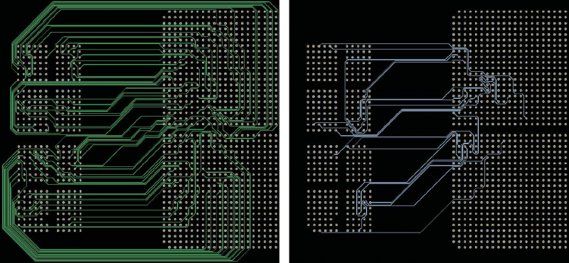
Routing one layer at a time. The first layer -green- contains 71 routes. The fourth layer, in blue, contains only 19 routes.
The routing shown above was performed sequentially, which causes one layer to fill up before the second layer. The figure below shows what happens when using the Altium auto router on both layers simultaneously.
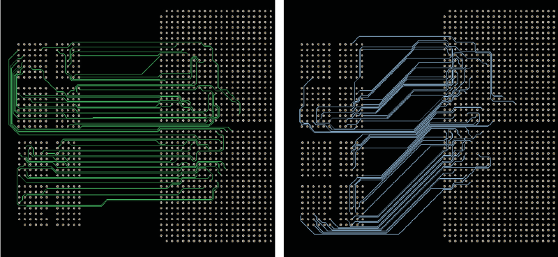
Routing on multiple layers simultaneously, resulting in a much more even distribution of traces. Layer 1 (green) has 48 routes and Layer 4 (blue) has 44.
In the context of time to route using these two methods, routing one layer at a time took 9m19s, while routing on multiple layers together took 0m:59s. Since the printed circuit board traces will be more evenly distributed when routing on both layers simultaneously, there will be more room for trace length tuning if required. If a routing algorithm struggles to make a completion, it adjusts the costs for each additional attempt to succeed. The method of routing on multiple layers eliminates this struggle, which makes it incredibly fast.
- Using an auto-router PCB tool is not always the best choice, and it depends on your layout strategy and components.
Learn more about autorouting and when it’s to use an auto-router.
- It’s important to understand how auto router algorithms work as this can help you plan the best way to incorporate PCB autorouting into your layout strategy.
Learn more about the algorithms used in modern auto routers.
- Other auto routers are stuck in the past, but Altium’s PCB Autorouter feature can help you easily automate portions of your routing and layout.
Learn more about the Altium's PCB Autorouter and how it will help you.
Auto-Interactive Routing Gives You More Control
As a PCB designer, you’ve probably worked with PCB autorouting before. You know the value of being able to complete the routing on your board much faster than you could when routing manually. You also know though that a typical PCB auto router typically produces results that are less than ideal and require some manual cleanup. There may be traces that are routed illogically, bus patterns that are scrambled, and the final routed results may require so much clean up that it would have been better to manually route it all in the first place.
This is where Auto-Interactive routing provides more control over routing. You can implement nearly any routing strategy you like, rather than constraining your routing strategy to comply with the settings in your auto-router. with Altium’s ActiveRoute tool, you’ll have an advanced user-guided router that automates trace routing between different points on your board. You simply select points for a group of nets on the board, and the auto-router portion fills in the rest with cleanly routed traces that satisfy your PCB design rules and constraints.
How Auto-Interactive Routing Works
Automated routing tools allow you to route signal nets extremely quickly while still ensuring that your device obeys critical design rules. Your PCB autorouting tools should make it easy to work with any combination of features on your circuit board, including routing through vias, across multiple boards, and with nets of differential pairs. Your automated routing tools should make pin swapping and part swapping simple while still preserving your differential pairs, controlled impedance, and conforming to your design rules.
With the ability to guide the routing path, ActiveRoute resolves one of the major problems in most PCB auto router tools. ActiveRoute allows you to guide the path for routed traces between different points on your circuit board, which gives you more control over your layout. This will help to organize your bus routing and direct routing away from areas that are reserved for other purposes.
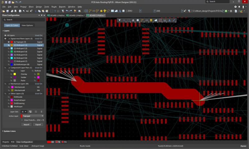
Auto-interactive routing in Altium Designer
Once you have finished routing, Altium Designer still has much more to offer. The high-quality CAD tools in Altium Designer give you the ability to visualize your board in 3D and import mechanical data into popular MCAD applications. You can visually verify your board and components will satisfy clearance constraints and that the circuit board will fit the system enclosure.
- High-quality design software doesn’t just place differential pairs, it ensures they obey design rules and can ensure signal integrity. Learn more about how strong design software aids differential pair routing.
- Your auto-interactive routing tools should allow you to route standard and advanced interconnect geometries. Learn more about choosing the right to interconnect configuration.
- With the point-and-click features in auto-interactive routing, you can easily navigate groups of traces around obstacles in your circuit board layout. See how auto-interactive routing helps you avoid obstacles in your PCB layout.
Advanced PCB Autorouter Features in Altium Designer
If you start routing directly in Altium Designer’s PCB editor, the PCB autorouting tool places traces using predefined design rules, such as trace/pad clearances and impedance tolerances. High-speed interfaces require meeting specific trace length tolerance rules, and high pin density components require pin-swapping capabilities that are powerful, yet intuitive. Differential pairs need to be routed in near-perfect harmony across your PCB layout. These design tools should work together and synchronize with your predefined design rules.
Automating the routing of each signal net ensures your layout complies with your design rules and gives you a precise trace arrangement. Just because you use layout software with a PCB autorouting tool doesn’t mean the results are set in stone. Powerful automated routing tools make it easy to adjust your layout if you ever need to swap parts, add new parts, or rearrange elements on your circuit board.
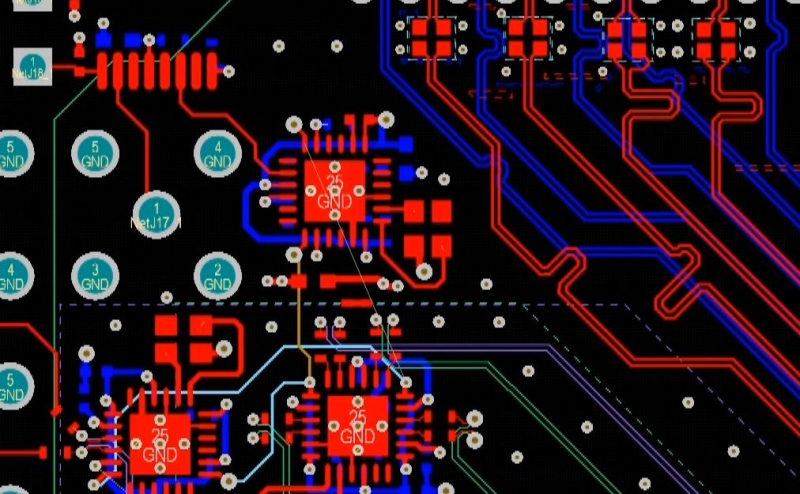
Differential pair routing with length tuning in Altium Designer
Altium Designer Offers Unparalleled Routing Accuracy
Low-end design packages can create common routing problems due to conflicting rules settings. Not only does poor design software route traces and differential pairs incorrectly, but you also won’t even be provided with the routing features unless you purchase them as add-ons. Who wants to route every single trace by hand, check length tolerances by eye, and insert meanders manually?
Altium Designer’s unified design environment provides a PCB editor with a powerful PCB auto router tool, the ActiveRoute module, and a host of other design features. You’ll also have access to a high-quality schematic editor, built-in simulation features, and a host of other synchronized features. These tools communicate with each other using a unified design model. This improves your workflow, catches design errors and rule violations quickly, and allows features to access information from each other.
- Altium Designer provides powerful CAD tools, PCB layout features, and routing features in a single design environment. Learn more about the circuit board design features you’ll find in Altium Designer.
- The ActiveRoute feature in Altium Designer is widely regarded as the most advanced yet easy-to-use auto-interactive router you can find. Learn more about ActiveRoute for Altium Designer.
- When you’re ready to begin designing your layout and routing, the integrated environment in Altium Designer makes it easy to transition from schematic to layout with a single program. Learn more about starting a new PCB layout in Altium Designer.
If working with separated PCB design software programs is hampering your routing strategy, you should try working in a unified design environment. Altium Designer integrates your schematic design, routing, simulation, and rules-checking tools in a single interface. You can rest easy knowing your PCB design tools will synchronize properly, and you’ll be able to prepare deliverables for manufacturing and assembly. No other software in a PCB auto router comparison can streamline this process like Altium Designer.
Forget about routing all your traces by hand. Altium Designer and the ActiveRoute package makes it easy to define your signal nets and quickly route traces between components. You’ll have access to the best design, routing, rules-checking, and simulation tools, all within a single design environment. Make the switch to Altium Designer today!

