Backplane Routing Topology for Gigabit Copper and Fiber Networks

Backplanes are the backbone of modular computing platforms, providing a fabric that interlinks pluggable daughtercards in a single system. The design of backplanes must support interfaces on the daughtercards, often at high data rates reaching multiple Gbps. Some standards also specify system design requirements that support RF or fiber integration into these systems. The RF and fiber portion is normally integrated through a specialized connector that interfaces with the transmission media, while the main backplane must support high digital data rates over copper.
Not all backplanes are standardized across multiple vendors, but those that are will specify some design requirements in terms of connector selection, pinouts, and routing channels. Whether you're designing for a standardized modular system (e.g., VITA standards in mil-aero electronics) or for a custom product line, these design guidelines will introduce you to the thought process involved in backplane design.
Some Backplane Routing and Design Requirements
There are some basic design aspects that must be considered for any high speed backplane, but the exact layout and construction of a backplane, including an optical backplane, will depend on the features used in your product:
- High speed protocols: Different connectors and channels are used to route connections between fiber/copper transceivers on daughter cards and the backplane. Your backplane will need to be designed around these possible connections and protocols.
- High voltage/current: Many backplanes run at high voltage, high current, or both. IPC standards should be the starting point for design and layout.
- Application: Your design should consider the proposed application; military and aerospace products will carry different performance/reliability requirements than a civilian product.
- Other peripherals: Backplanes can contain a number of other peripherals beyond high speed copper and fiber connections. These will need to coexist with high speed signals.
- Standard: The major standards groups used to specify backplane architectures are VITA and PICMG; these will give the functional design requirements for backplane routing and topology.
Before looking at your routing topology, you'll need to ensure the board is designed to support the data rates required between daughtercards. One of the first places to start is in connector selection and pinouts across connectors.
Separate Slow and Fast Signals in Backplane Routing
Any backplane might need to support a large number of signaling standards, ranging from simple SPI/I2C/GPIOs all the away up to multi-gig Ethernet and high speed SerDes channels. Today, 100GbE is common in newer daughtercards, and the backplane must be designed to support these data rates. When selecting which signals will go to which connector pins, try to set up the board so that slower signals are kept away from faster signals if placed on the same layer. The construction of standard backplane-to-daughtercard connectors and their pin arrangements enforce these requirements, as shown below.

When routing is dense, one strategy in a non-standardized backplane is to keep high speed differential signals on one half of the board and the slower single-ended signals on the other half. If the board is small (e.g., 1 or 2 U), you might not have such luxury and you'll have to increase your layer count to isolate signals. In VITA backplanes, for example, pin arrangements and channels are specified in such a way that it's easy to implement the above topology with differential channels routed between connectors. These are the so-called fat-channels, thin-channels, and ultra-thin channels.

By separating signals in this way, you can still touch all the connector pins as you route across the backplane, but you won't be inducing crosstalk from high speed to low speed signals. As we'll see below, this style still lets you satisfy a standard backplane routing topology when routing to fiber/copper transceivers and daughtercards. However, it can be challenging to get this perfect as these signals will come close to each other as they interface with various components.
How to Route Differential Pairs Between Connectors
The above image showing connector pins shows something important: the differential pairs need to be sized so that they can route between these rows of through-hole pins. The same idea applies if the positive and negative pins are arranged vertically. These pairs need to also be routed with impedance that matches the interface specification. What is the best way to make sure you always hit the impedance spec when routing through such narrow channels?
With the standard pin pitch being on the order of 2 mm, the spacing between pairs could be small enough that it will dominate the impedance profile of the differential pair. A pin pitch of 2 mm only leaves about a 1 mm wide routing channel after accounting for the pad size. You then have the available channel width reduced further due to clearances required between rows of pins on the backplane connector.
- Backplanes can have high layer counts, so thin layer counts (anywhere from 5-10 mils) are used to keep the thickness reasonable. The thickness is often non-standard.
- The clearance between pins will then require differential pair spacing that is rather tight, between 5 and 10 mils being an appropriate value.
- The narrow spacing and thin layer count will force traces in the pair to be thin as well. traces may be narrower for stripline routing.
Because copper-to-copper clearances could be more conservative in some standards, you will might need to use tighter spacing.
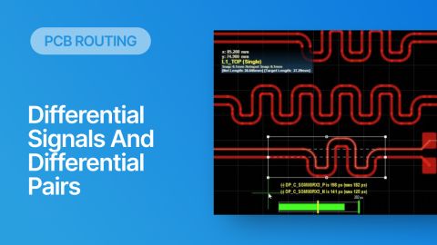
The result here is that you should maintain the coupling throughout the length of your routing channel. If the pair is designed with narrow spacing to hit an impedance target, then maintain that throughout the length of the route. The pinout you use and symmetric bending will help ensure you don't need to use length tuning sections as these will cause a deviation in the trace's odd-mode impedance. This then increases the losses you would expect in the channel.
Instead, you might expect to apply length tuning between pairs in multiple channels, such as if you need synchronization between daughter cards. An example is shown below.

Copper/Optical Backplane Routing Topology
Placing an individual transceiver in a daughtercard layout or some other high pin count components on the daughtercard are no trivial matter. The backplane for connecting multiple daughtercards along with their high speed links to copper/optical transceivers should be designed with a particular routing topology, depending on the components and signaling standards you need to use.
The principle backplane routing topologies used in modern products are point-to-point and point-to-multipoint. Point-to-point is probably the simplest routing style and it facilitates standard linear buses that are useful for routing across a backplane and touching multiple connectors. These backplane routing styles used to route connections within the standard backplane network topologies: star, double star, and mesh. The choice of backplane routing topology depends on the particular application and signaling standard used in your components.
Star and Double Star
A star network is probably the most popular topology used in networking. A star network on a backplane uses point-to-point connections between a central control unit (this could be on the backplane or daughtercard) and all other nodes (in this case, connectors). A double star network is just an extension of this, where two central nodes communicate with all other nodes, and with each other. Point-to-point routing is used for routing to other connectors, although a given connector node may branch off to other connectors in a point-to-multi-point manner.
Fully-Connected Mesh
The mesh topology is only useful when the number of line-card connectors and routing density are low. Point-to-point connections are still used to build connections between nodes. In other words, a mesh topology uses point-to-point routing to route each connector to all other connectors. For this reason, larger backplanes can facilitate a star or double-star topology unless mesh is necessary for the particular application.

Network topologies defined in VPX standards.
The optical portion of these systems will be brought in through fiber connectors that interface with a receiver, but the data routed over a fiber link will still need to be transferred over copper. The use of copper in these systems is unavoidable, even up to multi-Gbps speeds between daughtercards.
Beyond Backplane Routing Topology
There are plenty of other high speed design issues to consider in modern backplanes, and some design choices will cross over into RF territory. High speed backplanes take
- Noise and crosstalk: From a noise suppression standpoint, differential routing is preferable as it offers high suppression of common-mode noise. Be careful with differential crosstalk between high speed lines.
- Isolation and your stackup: As was mentioned above, high speed signals need to be isolated from low speed signals and each other. Connectors with more pins will generally require a higher layer count in the backplane to accommodate routing between connectors.
- Impedance control: When your PCB design tools include an integrated field solver, it's easy to account for copper roughness and dispersion when building an impedance profile for your high speed signals.
- Via stubs and via count: This is a matter of selecting the best routing tools and ensuring consistency in your connections. Via stubs will need to be limited and backdrilled to prevent any resonance in the via stub. Via counts also need to be limited to prevent excess return and insertion loss, including insertion loss resonances.
- Differential length tuning: For the high speed portion of the system, such as SerDes channels and Ethernet links, you'll need to apply very precise length matching as was discussed above. Make sure the pinout on connectors can support this.
If you’re in the business of designing backplanes and other designs requiring high speed data transfer over copper, look to Altium Designer® for a full suite of design and simulation tools for any backplane routing topology. The design and layout tools are ideal for applications in high speed networking, embedded computing, and other RF devices. The data management and documentation tools can help you quickly prepare your designs for prototyping and full-scale manufacturing.
Contact us or download a free trial if you’re interested in learning more about Altium Designer. You’ll have access to the industry’s best layout, simulation, and data management tools in a single program. Talk to an Altium expert today to learn more.


