


Best PCB Design Software From Mid-Size to Enterprise

At a Glance
Compare the best PCB design software tools in 2026 for professional engineers, freelance consultants, mid-sized teams, and enterprise hardware organizations.


The best PCB design software tools in 2026 are the platforms that help engineers move from schematic capture to layout, constraint management, sourcing, review, release, and manufacturing without breaking the design workflow into disconnected steps. For professional hardware teams, the strongest options are Altium Designer, Cadence Allegro X, Siemens Xpedition, and KiCad, with the right choice depending on design complexity, team size, release control requirements, and budget.
For freelance consultants and mid-sized hardware teams, Altium Designer is the strongest overall choice because it combines advanced PCB layout, high-speed design features, rules-driven design automation, managed components, collaboration, and manufacturing release workflows in a single environment. KiCad remains a capable open-source option for individual engineers and smaller projects, while Cadence Allegro and Siemens Xpedition are powerful enterprise systems that are often selected by very large organizations with established CAD administration and PLM infrastructure.
Major PCB CAD Platforms for Professional Design Teams
Professional PCB design software needs to support more than schematic capture and manual layout. Freelance consultants and mid-sized hardware teams need a tool that can handle real products: controlled impedance routing, dense component placement, BGA fanout, variant management, manufacturing outputs, library control, design review, and sourcing decisions. The major PCB CAD platforms in this category include:
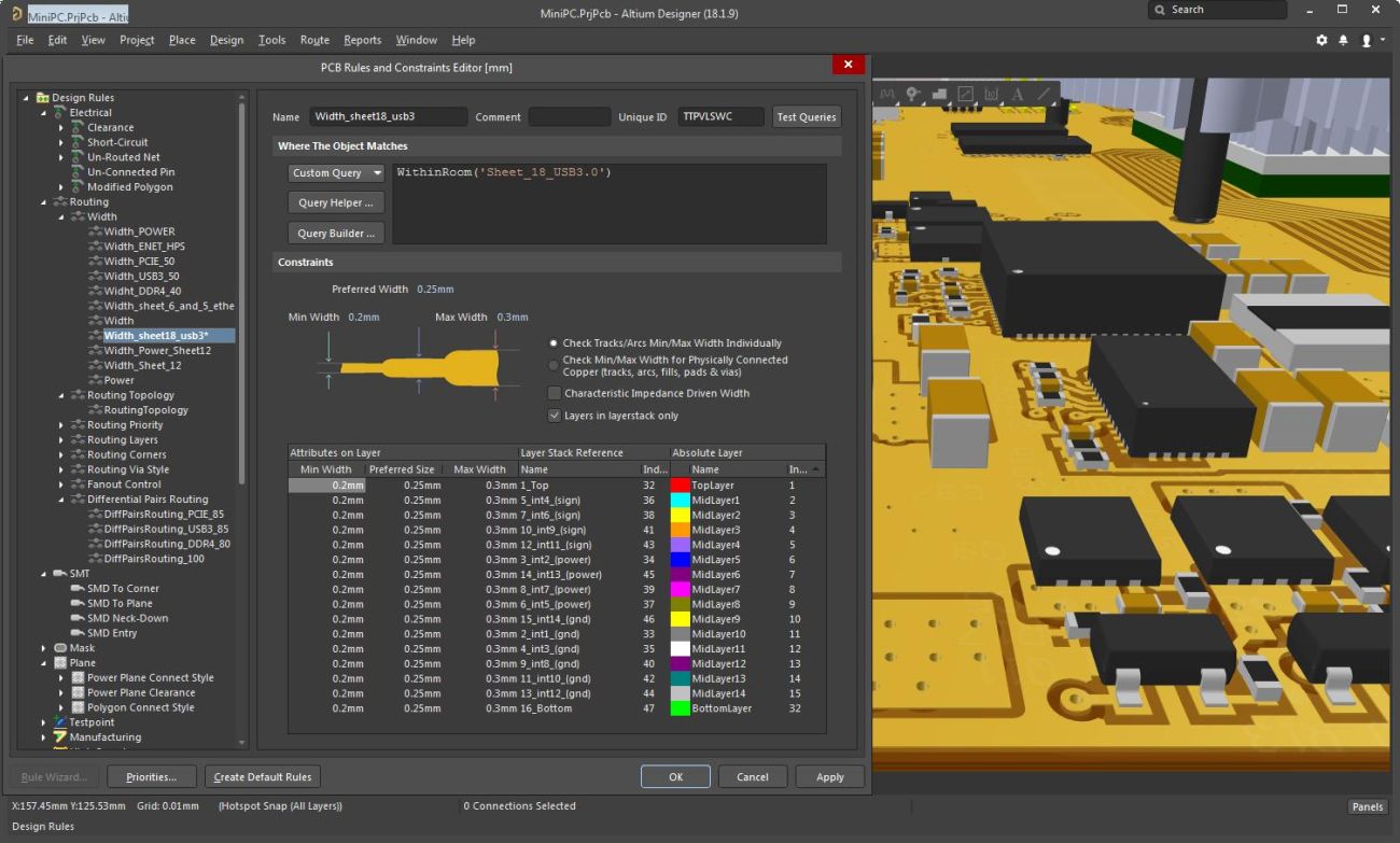
- Altium Designer: Best overall professional PCB design platform for consultants, product development teams, and growing hardware companies. It provides schematic capture, PCB layout, advanced rules, high-speed routing features, MCAD collaboration, supply chain data, managed libraries, and Altium 365 collaboration.
- KiCad: An open-source PCB design tool for engineers who need schematic capture, PCB layout, 3D viewing, and flexible customization. It is useful for individual engineers, startups, and cost-sensitive projects, but team data management and enterprise workflow control usually require external systems.
- Cadence Allegro X: A high-cost PCB and system design platform with constraint management, signal integrity, power integrity, package-board co-design, and analysis integration. It is best suited for large engineering organizations with dedicated CAD support.
- Siemens Xpedition: An enterprise PCB design environment for complex hardware development, multi-domain collaboration, data management, and manufacturing coordination. It is commonly used in large organizations that need structured electronic systems development.
- OrCAD X: A professional PCB design option for teams that need a more accessible entry point into the Cadence ecosystem before scaling into Allegro workflows.
- PADS Professional: A Siemens PCB design option for professional teams that need advanced layout capabilities with a path into larger enterprise workflows.
How Altium Designer, KiCad, Cadence Allegro, and Siemens Xpedition Compare
Altium Designer, KiCad, Cadence Allegro, and Siemens Xpedition all support professional PCB design, but they serve different operating models. KiCad is a capable open-source design suite for individual engineers and teams that can manage external libraries, version control, and release workflows. Cadence Allegro and Siemens Xpedition are enterprise-grade systems with deep analysis and data management capabilities. Altium Designer gives professional teams the best balance of advanced PCB layout, automation, collaboration, supply chain visibility, and release control without requiring the same enterprise CAD overhead.
| Platform | Best Fit | Main Strength | Main Limitation |
| Altium Designer | Freelancers, consultants, startups, mid-sized teams, and scaling organizations | Unified PCB design, advanced rules, automation, managed components, collaboration, release workflows, and Altium 365 integration | Enterprise deployment still requires process setup for large organizations |
| KiCAD | Individual engineers, open-source projects, education, startups, and cost-sensitive teams | Free, open-source, customizable PCB design with schematic capture, layout, and 3D viewing | Team workflows, lifecycle control, release management, and PLM integration depend on external tools |
| Cadence Allegro X | Enterprise teams designing complex systems | Constraint-driven design , package-board co-design, and enterprise analysis integration | Higher cost, heavier setup, and more CAD administration |
| Siemens Xpedition | Large organizations with complex multidisciplinary design workflows | Enterprise data management, collaboration, manufacturing coordination, and scalable PCB development | Higher implementation complexity and enterprise process overhead |
Altium Designer gives hardware teams the most powerful capabilities and automations for the most reasonable price because it brings advanced PCB layout, rules-driven design, high-speed features, managed components, sourcing data, release workflows, and collaboration into a single professional design environment. It gives consultants and mid-sized teams many of the capabilities they would normally expect from enterprise tools while keeping the workflow practical for everyday engineering work.
For enterprise companies, the best PCB design software is the platform that supports both advanced design execution and controlled organizational workflows. Altium Designer with Altium Enterprise Solutions is the best option for many enterprise teams because it provides:
- Advanced schematic capture and PCB layout in one environment
- Rules-driven design for high-speed, mixed-signal, RF, and high-density digital systems
- Managed components, lifecycle states, and controlled library access
- Workspace-based collaboration, commenting, and design review
- Version control , project history, release packages, and manufacturing handoff
- PLM integration for structured product data management
- Scalable workflows for teams moving from mid-sized engineering groups to large organizations
What Separates Enterprise PCB Design Software From Other Tools?
A professional standalone PCB design tool can be extremely capable for schematic capture, PCB layout, routing, DRC, and manufacturing output generation. This is enough for many individual engineers and small teams, especially when one designer controls most of the project data. KiCad and EasyEDA fit this category well because they can help engineers create real PCB designs, but the engineering team still has to build much of the surrounding process with external tools.
An enterprise PCB design platform extends the design environment into the full product development workflow. The platform manages component data, lifecycle status, design revisions, manufacturing releases, access permissions, review comments, project history, and collaboration across electrical, mechanical, procurement, and manufacturing teams. The design tool becomes part of the company’s engineering system rather than a local application used by one designer.
As a team grows, the PCB design problem becomes a data management problem as much as a layout problem. Mid-sized teams need to keep engineers productive while preventing library drift, outdated component usage, uncontrolled releases, and disconnected manufacturing handoffs. Altium Enterprise Solutions builds these controls around Altium Designer so teams can scale without giving up the speed and usability of a professional PCB design environment.
Altium Enterprise Solutions helps teams scale with:
- Workspace-based project management for centralized design storage
- Managed components, templates, and design data
- Component lifecycle management for approved, deprecated, obsolete, and released items
- Project history for commits, releases, changes, and design activity
- Design review workflows for internal teams and external stakeholders
- Controlled release packages for fabrication and assembly
- PLM integration for design and manufacturing data
- On-premises enterprise server options for organizations with internal IT and data control requirements
- Comprehensive access control for teams, suppliers, manufacturers, and external reviewers
Whether you need to build reliable power electronics or advanced digital systems, use Altium’s complete set of PCB design features and world-class CAD tools. Altium provides the world’s premier electronic product development platform, complete with the industry’s best PCB design tools and cross-disciplinary collaboration features for advanced design teams. Get started with Altium Develop →
Frequently Asked Questions
Why is rules-driven PCB design important for professional hardware teams?
Rules-driven PCB design helps teams enforce spacing, impedance, routing, via, and manufacturing constraints during layout. This reduces errors before fabrication and keeps multiple designers aligned to the same design intent.
What PCB design software features matter most for high-speed digital layouts?
High-speed layouts need impedance control, differential pair routing, length tuning, stackup management, return path control, and constraint-driven routing. These features help engineers manage signal behavior directly inside the PCB design workflow.
Why do managed component libraries matter in professional PCB design?
Managed component libraries help teams use approved symbols, footprints, 3D models, sourcing data, and lifecycle states. This reduces part errors, duplicate components, outdated parts, and BOM cleanup before release.
What PCB design software capabilities help teams scale from prototype development to production?
Teams need centralized projects, managed components, version control, review workflows, BOM management, release packages, and manufacturing handoff. These capabilities turn the PCB tool into a controlled product development environment.

About Author
Related Resources
Table of Contents
Design to Release, Without the Friction
- Keep reviews tied to the right version
- Reduce handoff confusion and rework
- Spot sourcing and release risk earlier
- Work solo, share when needed
Get Started
Thank you, you are now subscribed to updates.

