


Impedance Control: How to Specify Your Requirements for PCB Manufacturers

At a Glance
PCB manufacturing houses can easily accommodate impedance control requirements as long as you can specify requirements clearly. Here’s what to tell your fabricator.


That moment when you transition a board to manufacturing can be nerve-wracking, especially for new designs. In order to ensure your design can be produced reliably, you need to make sure you communicate a complete set of requirements to your fabricator and assembler. One of the important points that needs to be clearly specified before PCB manufacturing is impedance control targets. This helps prevent any confusion and helps you get through the design review process quickly.
How to Tell PCB Manufacturers Your Impedance Requirements
Like so many questions that get asked in PCB design, the answer is: it depends. Usually, the answer is “yes,” but if you do some homework on the front-end, your manufacturer won’t have to put in much effort to verify your impedance calculations.
All manufacturers need to do some level of front-end engineering to get your board into fabrication. Some of this will relate to verifying your stackup is manufacturable with their material stocks, which inevitably affects impedance. Some questions you might want to think about include:
- Are you requesting some design services from your manufacturer?
- Does the fabricator need to perform any testing or impedance measurements?
- What materials do they have in-house or through partners, and will these work in your design?
Sometimes, you’ll need to specify impedance depending on the service level you’re seeking from your manufacturer. The cheapest fabricators probably won’t even ask you about impedance, they’ll just produce whatever you give them with minimal review. In some cases, a design has been sufficiently qualified and tested that a manufacturer will need to perform a quick design review before putting the board into fabrication. However, they may still need to check your impedance against their stackup tables and available material stocks just to be sure they can reach your impedance target. At the highest service level, your fabricator is designing your stackup for you and will tell you what trace width you need to reach a desired impedance.
If you determine you need to specify impedance control requirements for a PCB manufacturer, there are a number of acceptable ways to do this.
Give Your Fabricator a Stackup Table
If you’ve created a complete stackup table, then you can include your impedance control spec as a note for your PCB manufacturer. You will typically want to include the following information:
- Trace width you’ve determined for a required single-ended impedance
- Repeat #1 for differential impedance
- Repeat #1 and #2 for each layer
- Specify these values for each transmission line geometry on each layer (coplanar vs. microstrip/stripline)
These points are important to specify clearly as different trace geometries may be present on different layers, and they might also have different impedance values. It’s important to be complete and clear in your PCB fabrication notes. Determination of all the trace widths required to reach impedance targets is one of the essential parts of front-end engineering that should normally be performed by designers. Using the right stackup calculator with an integrated field solver makes this easy.

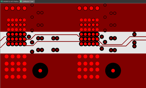
If you develop a stackup table for your board, make sure to add a note about the required trace width to hit an impedance target as shown above. The above image is an example where the prepreg thickness between layers 1-2 and between 3-4 have not been determined; the laminate and thickness will be determined by the fabricator while the design is reviewed. Not all fabricators will do this for you, which is why you should contact a fabricator that can support your desired layer stack and trace width to ensure you hit impedance targets.
If you started your project the correct way and you talked to your fabricator first, they will give you a stackup table that specifies trace widths required for a designed impedance. Assuming they approve your required materials or they stock a suitable substitute material, they’ll return a stackup that is calculated to meet your impedance requirements with specified trace widths and spacing (for differential pairs). When you create your stackup table in your fabrication drawings, follow the fabricator’s original stackup and include the impedance specification as a note next to the stackup table.
Specify Impedance in Your Fab Notes
This is what designers will often do when they only care about impedance matching, but they are not designing the board around their manufacturer’s material stocks. FR4-grade laminates and other materials can be substituted for each other, but this could require changes to the trace widths in your design in order to hit impedance goals. Typically, a designer will choose a material that conforms to a specific slash sheet, and that probably has a specific thermal property they care about. They will then use that dielectric constant to determine the trace width required for a specific impedance.
The impedance will then be specified using a note in a PCB fabrication drawing.
IMPEDANCE REQUIREMENTS:
1. ??? OHM IMPEDANCE REQUIRED FOR X.XXX MIL TRACES ON LAYERS X, Y, Z.
2. ??? OHM DIFFERENTIAL IMPEDANCE REQUIRED ON X.XXX MIL TRACES / X.XXX MIL SPACING ON LAYERS X, Y, Z.
This is fine as long as you know your fabricator can substitute alternative materials that will ensure the impedance in every layer can hit your targets. This is yet another reason to talk to your fabricator early; ask them for their standard stackups and design rules, and you’ll eliminate the need for design changes later.
Make an Impedance Table
One option is to place a small table in your fabrication drawing that summarizes all the impedance requirements on each layer. Again, you’re only specifying a single width and impedance value on that particular layer. This is either the impedance you determined from a stackup calculator, or it’s the impedance goal you need the fabricator to hit in your design. A simple (color) impedance table you can place in your fab notes is shown below.

Despite the ease with which designers can do a controlled dielectric PCB stackup design, impedance tables are still commonly supplied by design teams who are moving a board into fabrication, particularly when the design team does not have a specification for a particular PCB laminate product. Impedance tables are also used by manufacturers when they supply their https://resources.altium.com/p/when-use-standard-stackup-pcb-fabricationhttps://resources.altium.com/p/when-use-standard-stackup-pcb-fabrication in order to make things easy for their customers. To learn more about impedance tables and how they compare to the controlled dielectric approach, watch the following video.
Include it in an SOW
Small manufacturing runs with rapid prototyping services almost never ask for a statement of work (SOW). You generally just submit your design data through an online portal or via email, they’ll quote it, and put it into production as long as it passes some basic DFM checks. Larger orders will require a statement of work to be submitted by you (the customer), and the fab house will add their list of tasks and requirements for you to approve before beginning production.
When you’re starting the conversation with a PCB manufacturer, it doesn’t hurt to put together an SOW or a list of requirements that includes your impedance requirements just to make sure they understand. If you requested a comprehensive design review, they will check your stackup and routing to make sure you’ve hit the spec in your SOW.
What Else Do You Need to Specify?
Impedance requirements aren’t the only point you need to specify in a design, but it’s one of the important points for modern circuit boards. Aside from the lower-speed digital interfaces, you’ll need to design to an impedance spec and communicate this clearly. There are some other important points to specify in your design:
- Silkscreen dimensions
- Finish plating
- Units on board dimensions
- Total board thickness
- Finished copper weight (desired)
- Tolerances on board dimensions
- RoHS compliance requirement
- Depanelization requirement
- IPC 6012 Performance Specification Level
To help you prepare for PCB manufacturing and ensure impedance control requirements are met, use the Draftsman tool in Altium Designer®. When you’ve finished your design, and you want to release files to your manufacturer, the Altium 365™ platform makes it easy to collaborate and share your projects.
We have only scratched the surface of what’s possible with Altium Designer on Altium 365. Start your free trial of Altium Designer + Altium 365 today.

About Author
Related Resources
Related Technical Documentation
Table of Contents
Design to Release, Without the Friction
- Keep reviews tied to the right version
- Reduce handoff confusion and rework
- Spot sourcing and release risk earlier
- Work solo, share when needed
Get Started
Thank you, you are now subscribed to updates.


