Complete Guide to PCB Aging Test Methods for Electronics

A finished PCBA that will be deployed in the field should pass several tests to ensure reliability and stable operation. Industry standards specify multiple testing methodologies, performance requirements, evaluation metrics, even test fixtures that must be used to assess electrical behavior, thermal cycling resistance, long-term thermal stability, ability to withstand thermal shock, and much more.
With Altium Designer, you’ll have a complete toolset for documenting all aspects of your PCB layout before sending it in for fabrication and assembly. Documentation can be a difficult task, but Altium Designer’s fabrication documentation tools can help you streamline creation of test requirements, drawings, output files, and testpoint reports to ensure comprehensive testing. If you’re tired of continually rebuilding your documentation and manually entering your project data, try using Altium Designer, the industry’s best PCB design platform for professional design teams.
ALTIUM DESIGNER®
The industry’s best electronics design and simulation application for professional designers and PCB manufacturers.
The success of the electronics industry has depended on implementing a range of test methods and qualification standards, particularly during and after manufacturing. One important group of tests is a PCB aging test, where the lifetime of a board is simulated and the PCBA is checked for reliability. These tests are sometimes called thermal aging tests or burn-in tests as they are performed at elevated temperature, and sometimes under temperature cycling. They may be performed alongside thermal shock tests, mechanical shock tests, and electrical discharge tests, depending on the industry standards and safety regulations governing that particular product.
Purpose of PCB Aging Tests
The purpose of PCB aging tests is to gather data for assessing the long-term reliability of a PCBA that may be placed into continuous operation for over 100,000 hours (at least 20 years). These tests evaluate an entire PCBA, so they tell you the overall reliability of the bare circuit board, its components, solder and mechanical components, and any other materials used in the construction of the PCBA. Obviously, a PCBA cannot be tested for 20 years continuously, so test engineers will perform simulated life testing or other tests to evaluate long-term stability.
With performance requirements and fabrication requirements becoming more complex over time, so has the documentation process used by PCB manufacturers and design teams. With the right design software, a design team can quickly generate their test and fabrication data directly from their PCB layout. Important requirements like the reliability of solder joints, required PCB materials, use of conformal coatings, and a range of test methods can be specified within the project documents and easily shared with manufacturers.
Easily Specify Your Test Requirements in Your Project Data
When you need to quickly and easily specify your testing requirements, use the complete set of design and documentation tools in Altium Designer. You’ll have the tools you need to ensure your fabricator and assembler understand your design intent, and you can specify your test requirements to ensure high quality. You can also specify your PCB aging test requirements as your fabricator will use these to evaluate reliability in your components, circuit board materials, and solder requirements during assembly.
- Quality control and testing will begin during fabrication, normally with continuity testing to ensure opens and shorts match the data in your netlist.
- Initial board bring-up can be probed and evaluated with numerous test methods. A standard test is in-circuit testing, where the PCBA is probed to check required voltages and currents.
- Once a board is assembled, it’s time to run a PCB aging test so that boards with defective components and solder joints can be identified and removed from production.
Learn more about burn-in testing for electronics assemblies.

Altium Designer and Altium 365 allow you to specify your PCB aging test requirements alongside your circuit board design data and fabrication files.
PCB Aging Testing Technology and Methodology
There are four typical PCB aging tests, all of which are thermally driven in nature. These tests include:
- Burn-in testing: A method for identifying which components and/or assemblies will fail early using statistical techniques.
- Highly accelerated life testing (HALT): Here the goal is to stress a device until it fails in gross overoperation. This mimics overoperation in the actual environmental conditions where the device will be deployed.
- Highly accelerated stress testing (HAST): Similar to HALT in that the design is stressed until total failure.
- Highly accelerated stress testing (HASS): Uses the same environmental stresses as in HASS, but at lower levels, and typically after a complete HALT test is completed.
All PCB aging test methodologies follow a similar procedure:
- Hold a batch of PCBAs or discrete components at elevated temperature for a certain amount of time (typically multiple hours or days)
- Test the batch for defects or component failures
- Remove the failed parts and test the remaining components/PCBAs
- Continue this until the premature failure group has been identified
- Analyze the results statistically to identify a premature failure rate
- Inspect the failed parts to determine the root cause of failure
In the event an assembly defect, fabrication defect, or individual component can be conclusively identified as the cause of failure, it can be removed and the design can be modified before producing at higher volume. This helps ensure high-quality manufacturing and assembly while also reducing risk.
Easily Modify Your Designs With Altium’s Powerful CAD Tools
Altium Designer is the only PCB design platform that includes a complete set of CAD features alongside industry-standard fabrication preparation tools. No other design platform gives you a complete toolset for documentation and design in one application. Once you’ve received your test results, it’s a simple matter to modify your design with the best PCB layout software, and you can instantly regenerate your manufacturing output files in seconds.
- Some PCBAs will need a conformal coating due to the environment where they will operate. Once you select a conformal coating, make sure you specify its test and inspection requirements in your design documentation.
Learn more about the different types of conformal coatings for your PCBA.
- Functional testing is the final portion of evaluation before scaling to high volume. Once validated, production can be scaled and validated with automated test methods.
Learn more about functional testing of a PCBA after performing an aging test.
- When you need to document important fabrication and assembly requirements, you can use the Draftsman tool in Altium Designer to create your documentation directly from your PCB layout data.

The Draftsmand utility in Altium Designer allows you to specify all aspects of your fabrication requirements and performance requirements without using an external CAD program.
Document Your Test Requirements with Altium’s Toolset
Altium Designer is the industry’s premier circuit board design software package for a range of products and applications, but it also includes the industry’s best manufacturing documentation toolset. Whether you need to specify conformal coatings, PCB materials, lead-free solder requirements, or test methods, Altium Designer’s documentation features can help ensure your PCBA meets your quality and performance standards.
With the Altium 365 platform, every Altium Designer user can share their design data alongside their fabrication files, assembly files, and test documentation. This even enables unique test methods and strategies like hardware-in-the-loop testing before and after performing PCB aging tests. Only Altium 365 and Altium Designer create a single ecosystem where designers, manufacturers, and test engineers can work together to solve complex printed circuit board design challenges.
Stay Productive With Altium’s Rules-Driven PCB Design Software
All of the PCB design features in Altium Designer were built to work together in a single, unified design interface. The underlying rules-driven design engine allows all your design and documentation features to share data and work together seamlessly. No other PCB design application helps you stay this productive and build advanced electronics.
- When you need to use the best design features for design documentation for your printed circuit board, look to Altium Designer, the industry leader in PCB design and manufacturing.
Learn more about Altium Designer’s complete circuit board toolset.
- Don’t use a separate application to specify your PCB materials and components testing and performance requirements. Altium Designer gives you everything needed for circuit board design and fabrication.
See Altium Designer’s complete set of PCB design tools in action.
- Once you’re ready to push your design, test, and manufacturing data to your fabrication and assembly team, you can use the Altium 365 platform. Every Altium Designer can use Altium 365 to push their project data to their manufacturer via a managed cloud platform.
Learn more about sharing your PCB manufacturing and test data with Altium 365.
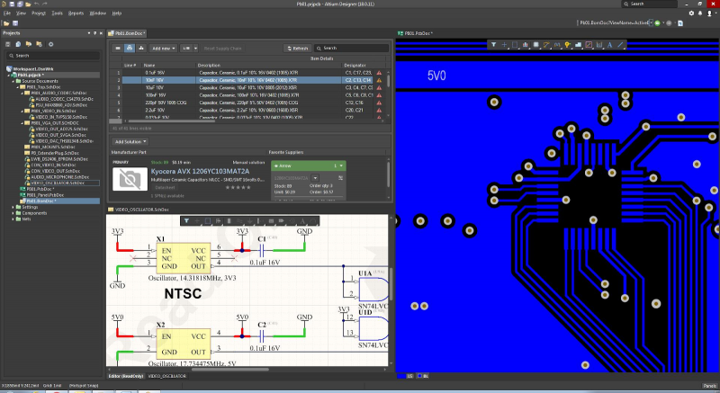
Altium Designer includes everything needed to design high-quality PCBs and prepare them for full-scale production in a single application.
With a full suite of professional documentation features, Altium Designer gives all users the ability to compile a complete set of test and measurement requirements, as well as PCB aging test requirements. These requirements can be easily created, compiled, and pushed to manufacturing with a single toolset in a unified environment. Forget about using multiple programs for design, layout, and simulation, use the industry’s best set of PCB design tools in a powerful application.
Altium Designer on Altium 365 delivers an unprecedented amount of integration to the electronics industry until now relegated to the world of software development, allowing designers to work from home and reach unprecedented levels of efficiency.
We have only scratched the surface of what is possible to do with Altium Designer on Altium 365. You can check the product page for a more in-depth feature description or one of the On-Demand Webinars.


