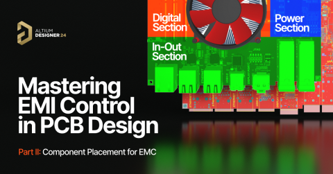


Mastering EMI Control in PCB Design: How Signals Propagate in a PCB


Mastering EMI Control in PCB Design Series
1
How Signals Propagate in a PCB
| August 29, 20242
3
4
5
6
Designing Printed Circuit Boards (PCBs) for Electromagnetic Compatibility (EMC) requires a solid understanding of signal propagation from the perspective of electromagnetic fields and currents. These concepts are important because they help us design PCBs with low levels of electromagnetic field emissions and low susceptibility to external emissions or interferences.
In this first article of the Mastering EMI Control in PCB Design series, we will dive deeper into these concepts and see how to apply them to Printed Circuit Board Design.
Concept of Signal Propagation in a Transmission Line
When thinking about how a signal propagates in a PCB, it's important to shift from the analogy of water flowing through pipes to thinking in terms of electromagnetic fields and transmission lines. A transmission line is a structure designed to transfer energy in the form of contained electromagnetic fields from one point to another. In the context of printed circuit boards, the transmission line is formed by at least two conductors. Both conductors are equally important in containing the electromagnetic fields and guiding them from one point to another in the circuit. If one of the two conductors is missing, the electromagnetic fields, which compose the signals, are left uncontained, potentially resulting in EMC test failures due to the expansion of these fields.
A very important concept that emerges from this is that the electromagnetic signal is not contained inside the conductor but in the space between two conductors, in the dielectric, and surrounding it. Our goal in terms of EMC is to maximize the electromagnetic fields contained between the two conductors and reduce the electromagnetic fields surrounding it.

Figure 1 - Representation of a digital signal propagation in a PCB
In PCBs, the two conductors used for signal propagation are the signal potential conductor and the return and reference potential conductor. The easiest way to picture this is in a two-layer board where the top layer connected to the signal source is used to route the signal traces, and the bottom layer is a solid copper layer connected to the signal source but also to the signal potential reference (See Figure 1). What we call a signal is the electromagnetic field contained between these two conductors. This means that the signal is not contained in a single conductor but is the electromagnetic energy contained in the dielectric between these two conductors. This also means that the properties of the dielectric material influence the propagation of the signal, particularly its influence on the speed with which the signal (or EM wave) propagates, which is the speed of light in the dielectric. There will be points between the two conductors where the signal is present and points where the signal has not yet reached. In a digital signal, the point between these two zones where we have the full signal and where we have no signal yet is called the signal edge or signal wavefront. This is the point of transition from low-level logic to high-level logic in the digital signal.
In terms of EMC, this point is extremely important because this is where the electric and magnetic fields transition from low to high between the conductors. The faster this state of energy changes, meaning the faster the signal transitions from low to high logic level, the more energy change is compressed in a short amount of time. As the signal propagates from its source to its destination in the transmission line, the signal wavefront or signal edge leads the propagation of the signal.
Forward Current, Return Current, and Displacement Current
Another important concept is that if we were to follow the signal edge as it propagates, we would see that since the leading edge is a change of the electromagnetic field, this would generate a displacement current in the dielectric between the two conductors. This phenomenon is explained by the four Maxwell’s equations put together by Oliver Heaviside, particularly the Ampere-Maxwell law. The easiest way to picture this is by thinking about how the current flows through a capacitor when an AC source is applied (See Figure 2).

Figure 2 - Capacitor (a) with no E fields applied (b) positive E field applied (c) negative E field applied
In reality, there is no conduction current between the plates of the capacitor and its dielectric, but the bound charges contained in the dielectric simply polarize (displace) following the applied fields of the capacitor's plates. This will appear as if a conduction current is flowing through the capacitor plate. The concept of displacement current is important for us to understand how it is possible for a current to form during signal propagation, especially before it reaches the load. As taught in classical circuit theory classes, the current always flows in loops. So how is it possible that we have a current even before the signal reaches the load and therefore before it establishes a continuous conduction current that goes from the source to the load and then back to the source to form the current loop? This is possible because of the displacement current, which allows the current to still flow in loops as the signal propagates. Without the displacement current, only having the conduction current, we would not have signal propagation, as the current loop made only by the conduction current would not be able to close the loop before reaching the load. This would mean that a conduction current would have to flow through the dielectric, which by definition is not possible. But with this apparent current, the displacement current, the loop is closed instantaneously as the signal propagates.
The combination of conduction current and displacement current will result in a current loop that propagates following the signal edge. This current loop, as shown in Figure 3, can be divided into three portions:

Figure 3 - Current loop and Displacement current
- The forward current, which flows in the direction of the signal towards the load on the conductor on the top layer.
- The return current, which flows in the opposite direction of the signal back towards the source on the bottom side conductor.
- The displacement current, which bridges the other two portions of the current by “flowing” through the dielectric between the conductors and following the signal edge.
Containing the Energy of the Signal for Controlling EMI
Managing the containment of electromagnetic fields between conductors and controlling the current flow path is extremely important for designing PCBs that not only outperform but also excel in electromagnetic compatibility and signal integrity (See Figure 4).

Figure 4 - Example of an advanced PCB design with Altium Designer® 3D viewer
This approach allows us to control emissions at their source and avoid designing PCB structures that permit the coupling of external interferences.
In the next article of the series, we will discuss how to improve component placement to effectively reduce EMI. To ensure you don’t miss it, stay tuned by following our pages and social media.
Conclusions
To design PCBs that meet these high standards, you need advanced tools that provide precise control over every aspect of your design. Altium Designer® offers a complete set of PCB design layout and simulation features, ensuring your designs meet all design requirements. The integrated design rules engine and online simulation tools help verify conformance to your design specifications as you route your PCB.
When your design is complete, seamlessly release files to your manufacturer using the Altium 365™ platform, which simplifies collaboration and project sharing.
You can start your free trial of Altium Designer + Altium 365 today and bring your PCB designs to the next level.

About Author
Related Resources
Related Technical Documentation
Table of Contents
Design to Release, Without the Friction
- Keep reviews tied to the right version
- Reduce handoff confusion and rework
- Spot sourcing and release risk earlier
- Work solo, share when needed
Get Started
Thank you, you are now subscribed to updates.

