

Mastering EMI Control in PCB Design: Crosstalk Prevention for better EMI


Mastering EMI Control in PCB Design Series
1
2
3
4
5
6
Crosstalk Prevention for better EMI
| February 27, 2025Welcome to the sixth article in the series, Mastering EMI Control in PCB Design. In this article, we will explore how crosstalk can affect both signal integrity and EMI, and discuss what steps to take to address this in our designs.
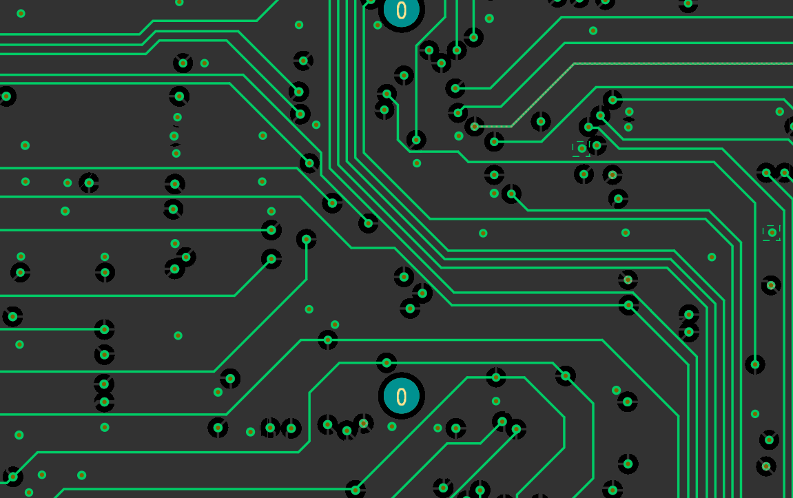
Figure 1 - Example of PCB Design in Altium Designer®
Crosstalk is one of the most frequently encountered issues in modern Printed Circuit Board (PCB) designs. As the density of PCBs continues to increase, this phenomenon is becoming even more prevalent. The trend towards integrating more high-speed interfaces into ever-smaller areas of the board exacerbates the challenge, as compact layouts lead to closer proximity between traces, which significantly raises the likelihood of crosstalk.
In essence, signal crosstalk refers to the unintentional transfer of an electrical signal from one net (or trace) to another. This occurs when the electromagnetic field generated by a signal traveling along one trace interacts with an adjacent trace. In this context, the trace carrying the original signal is commonly referred to as the "Aggressor", while the trace that receives the undesired signal is known as the "Victim".

Figure 2 - Example of how crosstalk can manifest in a circuit
In the field of electromagnetic interference (EMI), crosstalk becomes very important because it can not only be the cause of interferences within a system, but it can also become the source of electromagnetic emissions that disturb other devices. What is important to see regarding crosstalk is that it not only happens between the signal traces, where the signal current propagates, but it also occurs at the return reference conductors, where the return current flows back to its source. This is where phenomena such as “ground bounce” occur, which is also a case of crosstalk that happens in the return reference conductor.
Understanding Crosstalk and Its Effects
The phenomenon of crosstalk occurs for two main reasons: capacitive coupling and inductive coupling between conductors. When two or more traces are routed too close together, and when a signal voltage and current change over time, the fringe fields (electric and magnetic fields) at the edges of the signal traces (called the Aggressor) can couple to the nearby traces (Victims), resulting in unwanted noise on these nearby traces.
The job of the PCB designer, in terms of reducing crosstalk and effectively reducing EMI, is to minimize the effects that these fringe fields have on other conductors, so that noise does not propagate from one trace to another.

Figure 3 - Example of inductive and capacitive coupling between signal traces
In terms of EMI, this becomes a problem when the noise generates emissions either from the PCB traces, or from the wires connected to these traces, or conductors.
Types of Crosstalk
When dealing with crosstalk, it is also important to distinguish between two types: Near-End Crosstalk (NEXT) and Far-End Crosstalk (FEXT).
Near-End Crosstalk, also called NEXT, is the type of crosstalk that occurs at the same end of the transmission line where the signal is transmitted. Essentially, it is the interference picked up by a nearby conductor at the transmitting end of the circuit.
Far-End-Crosstalk, or FEXT refers to crosstalk that occurs at the opposite end of the transmission line from where the signal is transmitted. It is the interference picked up by a nearby conductor at the receiving end of the circuit. The key difference is that NEXT occurs near the source end, while FEXT occurs near the destination end. NEXT happens in the reverse direction of the signal propagation (backward direction), whereas FEXT happens in the direction of the signal propagation (forward direction).
Practical examples and layout strategies in Altium Designer®
Without going too deep into the complexities of signal crosstalk, which could fill an entire series, there are several ways to reduce its effects. Most of these techniques are dependent on the way we design the PCB layout, which means that the way we geometrically design the PCB becomes very important. The most effective ways to reduce crosstalk are, in fact, related to how we dispose of the conductors relative to each other on the PCB.
One of the first strategies we can use is to increase the space between the conductors so that the electric, and magnetic fields, do not couple with each other.

Figure 4 - Example of signal trace spacing before and after the improvement
Another technique that we can use is to reduce the space between the signal traces and the return reference plane. This will tightly couple the signal fields with their return reference planes, reducing the spreading of these fields to other conductors.
Also, reducing the length of both conductors, the signal conductor and the return reference conductor, will reduce the amount of coupling between different nets. This is also intuitive, as the less the conductor is exposed, the less chance the noise has to couple with other conductors.

Figure 5 - 3D view of tightly coupled signal and return reference planes with Altium Designer®
Another common method to reduce crosstalk, which is effectively applied to ICs, connectors, and PCB traces, is to provide multiple conductors for the return path of different signals.
This means, for instance, using multiple return paths when using ribbon cables or other connectors, instead of using one single return conductor for multiple signal nets.
Simulation strategies with Altium Designer®
Instead of relying on educated guesses about crosstalk in our circuit layout, it’s important to use advanced tools for precise calculations.
The Signal Integrity feature embedded in Altium Designer® is a powerful tool for this purpose. This feature allows us to simulate and analyze crosstalk across PCB traces, enabling accurate predictions and a deeper understanding of crosstalk levels. By using this tool, we can refine and optimize our design with greater precision.

Figure 6 - Example of crosstalk simulation using Altium Designer®
The Signal Integrity tool provides detailed simulations that help us evaluate various design trade-offs. Understanding these trade-offs is essential for minimizing interference and achieving optimal performance. The insights gained from this tool are far more reliable than those obtained through guesswork alone.

Figure 7 - Example of crosstalk evaluation using the Signal Integrity tool in Altium Designer®
Leveraging this advanced tool helps us make informed decisions, balancing performance needs with layout constraints. This approach enhances both the reliability and functionality of our circuit, improving signal integrity and EMI performance while increasing overall design efficiency.
Conclusion
In conclusion, to effectively reduce signal crosstalk and improve the EMI performance of our PC boards, we have several strategies at our disposal. The use of Altium Designer's embedded Signal Integrity tool is indispensable for accurately predicting and mitigating crosstalk in our PCB layouts. This tool empowers us to make data-driven decisions, ensuring that our designs meet the required specifications and perform reliably under various conditions.
If you have happened to miss any of the previous articles in the comprehensive "Mastering EMI Control in PCB Design" series, we highly encourage you to visit the Altium pages to catch up on all the insightful content.
Additionally, make sure to follow Altium on their various social media platforms to stay updated with the latest news, articles, and updates related to PCB design.
If you are seeking ways to enhance and elevate your PCB design projects, and if you wish to take full advantage of advanced tools that can significantly simplify and streamline the design process, we strongly recommend that you consider starting a free trial of Altium Designer® and Altium 365™.
These cutting-edge tools offer a range of powerful features designed to improve the efficiency and effectiveness of your design workflow, making it easier to achieve high-quality results in your PCB projects.

About Author
Related Technical Documentation
Table of Contents
Design to Release, Without the Friction
- Keep reviews tied to the right version
- Reduce handoff confusion and rework
- Spot sourcing and release risk earlier
- Work solo, share when needed
Get Started
Thank you, you are now subscribed to updates.

