ESD Grounding Requirements in Your Next PCB

Any PCB that will be deployed in an environment surrounded by high voltage equipment or power sources is at risk of electrostatic discharge (ESD). Static electricity can also discharge directly into a board and ruin sensitive electronic components if a board is handled without a wrist strap. This induces a transient voltage in the PCB, which can cause damage to sensitive components. In extreme cases, such as lightning strikes or major power surges, ESD and transient voltages can cause a board to catch fire, similar to what happens when a circuit shorts.
Given the dangers associated with ESD, many industry standards define ESD grounding requirements for protecting sensitive circuits. With the right design software, you can implement measures to protect your circuits from damage by following the right ESD grounding requirements. Altium Designer contains the important tools you need to create a grounding floor plan that can provide the right level of ESD protection required for your application.
ALTIUM DESIGNER®
A PCB design package with the best schematic design, component management, and layout features in a single software platform.
Lightning strikes, power surges from your local utility, shorts in your home electrical wiring; all of these can be protected with a surge protector. You likely already use power strips in your home electronics, so you’re familiar with the surge protection they provide. A surge protector will dampen the current spike induced in your electronic products, protecting them from damage. Your home circuit breaker includes a switch that automatically triggers in the event of a short circuit, protecting your home from an electrical fire.
The transient voltage and current spikes induced in all of these systems can happen in devices that are not connected to a 110 V or 220 V AC line. Many industry standards require that PCBs for electronic products include transient voltage suppression mechanisms. The acceptable limits for power fluctuations and transient voltages due to ESD are defined using the CBEMA curve, and this curve forms the cornerstone of many industry requirements.
There are several methods you can implement in your boards to protect them from damage due to ESD. Arguably, the most effective strategy is to protect your components from damage by implementing the right ESD grounding strategy. No matter which method you choose, you’ll need to work with design software that makes it easy to implement these protections at the PCB level. This goes beyond simply planning to use a surge protector or a circuit breaker to protect electronic equipment.
ESD Grounding Methods for Shock Management
The simplest and yet most effective method for suppressing transient voltage and preventing sensitive circuits from ESD is to cut power from the circuit in the event of a spike. You can use a circuit breaker or a fuse for this strategy, but it relies on placing one or more of these elements in the right place in your board. Clearly, this quickly becomes impractical given the numerous other requirements that most designs carry.
The best application of ESD grounding requirements to shock management involves protecting your board from ESD that travels directly to your board from an external source. A better option is to design a grounding strategy that routes any discharge from static electricity to an electrical ground. This prevents any induced voltage from passing a current into your components.
Designing Your Board With a Grounding Strategy
Implementing a grounding strategy takes more than just placing a ground plane in your board. If static charge between two points induces ESD directly into your ground plane, current can travel directly to sensitive components that are connected to the ground plane. A transient voltage induced in the board tends to be quite strong, driving and inducing currents elsewhere in your board that can damage components.
Thankfully, there are some components you can install alongside your ground plane to protect sensitive electronics from an ESD event. Two important components are TVS diodes and bypass capacitors. When properly combined with a ground plane and a larger grounding strategy, you can meet ESD grounding requirements for your device.
- ESD can arise from a number of external sources and is important in many electronic devices. Learning more about the causes of ESD can help you implement the right design to protect your circuits against an ESD event. Learn more about ESD and some protection measures for your PCB.
- Simply placing a ground plane somewhere in your board isn’t enough to suppress every ESD event. Learn more about using a PCB ground plane for ESD protection.
- Once ESD occurs, the quick flow of current and a transient voltage signal can induce currents elsewhere in your circuit due to parasitic inductance. Some clever design choices can help your circuits withstand ESD. Learn more about the relationship between ESD and parasitic inductance in your PCB.
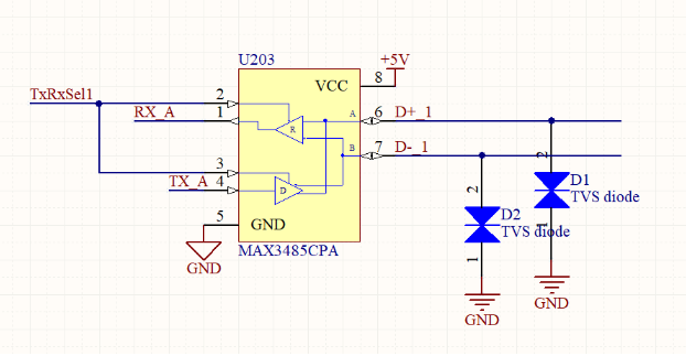
Placement of a TVS diode in an electronics schematic
Component and Chassis Grounding for ESD Protection
Whether you are deploying a board near other high voltage sources or you just want to protect your board from static electricity, the right grounding strategy will divert currents away from sensitive components and back to a grounding point. Aside from placing a ground plane in your PCB, some smart component placement strategies will provide your components with significant ESD protection. In addition to the use of bypass capacitors and judicious use of TVS diodes, trace lengths between components should be as short as possible to minimize parasitic inductance.
Perhaps the best grounding strategy is to attach a connection between your ground plane and the chassis for your device. This allows any current spike due to an ESD event to travel back to ground through a bulky metal chassis, eventually reaching earth. This allows an induced current to flow through your ground connection and away from your board, rather than flowing through sensitive components.
How to Check ESD Grounding Compliance for Shock Management
Using components by themselves is not a cure-all for ESD problems, and the same applies to a ground plane in your board. Instead of relying on components or grounding on their own, your design software should allow you to implement both strategies to protect yourself from ESD. With the right software, you’ll be able to find and place the right components for strong ESD protection, as well as design a grounding strategy for your board.
When your PCB design software includes power simulation tools alongside your design features, you can immediately simulate the response to a transient voltage in your board. The response in different signal nets or traces can then be compared to the electrical ratings for your components, allowing you to determine the effectiveness of your ESD suppression strategy.
- Once you’ve added the right components to your layout and finished your ground plane designs, you can check for ground loops, potential thermal problems, and islands or peninsulas using a PDN analyzer. The right PCB design software includes this alongside your design features.
Learn more about examining your grounding strategy with a PDN analyzer.
- With the right simulation package, you can perform transient analysis and determine the effectiveness of your ESD protection strategy. Learn more about transient analysis in your PCB design software.
- PDN analyzers reveal a significant amount of information about your power distribution network in a single simulation output. Spotting the signs of PDN problems takes some experience, but Altium provides you the resources to work with this powerful tool.
Learn more about the signs of a bad power distribution network in your PCB.

Designing and placing a copper region in Altium Designer
Designing ESD Protection With the Best PCB Software
How can the right software help you implement a strong grounding strategy? Aside from placing components, placing a ground plane, and defining ground connections to a chassis, the best PCB design software will take this data and feed it directly into simulation and verification features. You shouldn’t have to switch to a different program to simulate the effectiveness of your ESD protection strategy. With Altium Designer, your design tools integrate directly with your simulation and analysis features in a single interface.
Altium Designer: Design and ESD Simulation Features in a Single Program
The days of switching between programs for essential design and analysis tasks are over. When your design, layout, and analysis tools are accessible within a single program, you can easily identify design problems that create vulnerability to ESD and correct them within a single program. You won’t have to export and import data between ESD control programs when you work with Altium Designer. No other PCB design software program offers this level of adaptability.
- The component search and management features in Altium Designer let you place and procure the right components for ESD protection. Learn more about the component management features in Altium Designer.
- Examining the effectiveness of your ESD protection strategy takes simulation and analysis tools that interface directly with your design data. Learn more about the PDN analyzer extension in Altium Designer.
- Ground plane design for your PCB requires CAD tools that are built into your design software. You shouldn’t have to export your board to a command line-based CAD program for such an essential design step. Learn more about efficient polygon design practices in Altium Designer.
The layout and component management features in Altium Designer are all accessible within a single program and allow you to implement any strategy to meet your ESD grounding requirements. You won’t have to switch between separate programs to implement a grounding strategy or access the components you need to protect your board from ESD. No matter which industry you work in, Altium Designer has the tools you need to incorporate ESD protection for any PCB.
Unified design helps you remain productive by placing all your features in a single environment with a consistent interface. If this design workflow is unfamiliar, Altium will be there with resources to help you reach success. You’ll have access to the AltiumLive forum, a knowledge base with useful design tips, and webinars and podcasts with design experts. Altium gives you all the resources you need to design successfully.
No other design platform includes the important schematic and layout features for PCB design. These features are placed alongside component management and verification tools within a single program. Instead of using multiple ESD control programs with inconsistent workflow and separate feature sets, you need to work with the only integrated PCB design software platform. Design your next PCB with ESD protection with Altium Designer.

