


EMI and EMC Compliance 101 for PCB Designers

At a Glance
Learn about the basics of EMI and EMC compliance requirements in PCB design and electronics product design.


EMI and EMC are two areas where PCB designers have an important role to play. The PCB designer’s job is to ensure a design is laid out such that noise generation is below regulatory limits. Many systems that are initially designed to be perfectly functional will not pass regulatory standards due to particular practices in the PCB layout. It then becomes the PCB designer’s job to modify a PCB layout to ensure it passes regulatory standards.
To help prevent repeated rounds of EMC compliance testing, redesigns, and prototype spins, there are some simple steps that designers can take to help reduce the occurrence of excessive EMI in the PCB layout. Some of these factors happen at the circuit level, and they should be addressed in front-end engineering and schematic capture. However, even a perfect circuit design can fail EMC testing if the PCB layout is not engineered correctly. This guide will focus on the factors in a PCB layout that can lead to EMC compliance failures.
What is EMC Compliance?
Every design that is intended to go to market at high volume will need to have low noise emission during operation. Emissions can be conducted away from the device (through cables) or radiated away from the device. There are limits on both types of emissions that are specified by regulatory authorities, as well as industry standards groups. EMC compliance also centers around ESD and the ability of electronic devices to withstand transients.
The table below outlines broadly what is tested under worldwide EMC regulations and industry EMC standards. This list is not intended to reference specific regulations, only the broad areas and types of tests that are performed for a new product.
|
|
|
|
|
|
|
|
|
|
|
|
|
|
|
|
|
|
|
|
|
|
|
|
|
|
|
|
|
|
Not all equipment will need all of these tests. For example, a device running only on battery power would not need to pass the voltage dips and interruptions test, so there is no need to design the board to those operational requirements.
Passing these tests is a regulatory matter, and there are companies who specialize in testing electronics to ensure compliance with regulatory requirements. These tests are not cheap; in the U.S. a single round of testing can cost on the order of $10,000. Companies cannot afford to spend money repeatedly on testing, so they have to learn to spot potential failures before sending a design out for testing.
Most Common Reasons for EMC Failure in PCB Design
EMC failure in a PCB layout often boils down to a small number of reasons, and it is the test engineer's job to track down the root cause of the failure. Some of these issues can be easily solved by changing the layout, routing, and/or PCB stack-up.
- Insufficient coplanar ground and/or no ground plane
- Use of multiple grounds for isolation between signals when not necessary
- Reception or emission of radiation from cables and connectors
- Radiation from routing without a consistent ground reference
- Radiation from fast-switching circuits where the ground has been removed
- Switching noise from a digital PDN supporting fast processors
- Radiation from a digital PDN requiring high bandwidth where ferrites are used
- In some cases, lack of board-level shielding for certain circuits
- Emission or reception of radiation from large sections of floating metal
- Incomplete return current path, leading to radiation often at high frequencies
- Failure to direct ESD currents away from unprotected components
- High impedance return paths between shield, chassis, and/or earth
- Noise in return paths coming to AC mains inputs, requiring a PFC (Power Factor Correction) circuit
The above is not an exhaustive list, but it covers many of the common instances in power and high-speed digital circuits, as well as some cases involving cabling and enclosures. Many EMC failures resulting from excessive EMI are due to some variants of the situations listed above.
If your role is that of a test engineer, particularly someone working on pre-compliance, your job is to hunt down and eliminate all possible causes of excessive EMI, which could lead to EMC testing failure. It is very important to address these potential failure mechanisms sooner rather than later; hence, the need for some level of pre-compliance testing. An EMC testing failure will almost always demand some level of redesign to the system, which translates to lost time and money for your company.
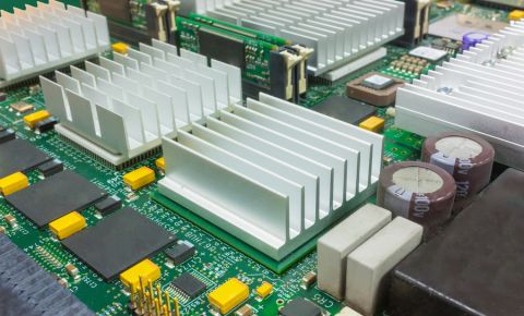
Within the above list, I have found that problems with insufficient grounding or the use of multiple disconnected grounds are the most common reasons for EMC testing failure. For example, take a look at what happens in a dense two-layer PCB. When two-layer PCBs have dense component placement and routing, many signals will lack sufficient ground and will create a lot of radiation. This is one of the primary motivators for switching to a four-layer PCB.

Arduino PCBs are great examples of layouts that are nearing the limit of component density.
Due to the potentially high level of radiation in this PCB layout, using a four-layer PCB stack-up would be a simple way to help ensure the design passes EMC testing without any other major design changes. It is often the case that EMI problems start in the stack-up and become system-level problems, so simple changes like adding plane layers could be a fast way to get your design through EMC testing.
Designing to Ensure EMC Compliance
Designing a PCB to ensure EMC compliance requires a bit of a change in thought process. Specifically, you need to see the match between “noise” in the PCB layout, a “radiator” as defined in EMC standards, and any area where noise could couple out of the system through a cable. An early recognition of this will help you spot potential EMI/EMC errors before you send a design to testing.
Layout and Routing
Layout and routing can influence the noise characteristics of a circuit, even if a circuit was optimally designed to reduce noise. This occurs through parasitic coupling between noise sources and circuits, or between circuits and free space. This issue with parasitics involves multiple aspects that are difficult to summarize into a single article. At a high level, there are two approaches to layout and routing that address parasitics:
- Capacitance - Tighter coupling to ground is the simplest way to suppress capacitive coupling between circuits.
- Inductance - Tight layout with shorter paths between components will reduce loop inductances that allow for radiation
For example, in power regulators, this greatly reduces noise coupling to the output of the circuit and into free space. An example that illustrates the tight routing concept with ground on L2 (including below the inductor) is shown below.

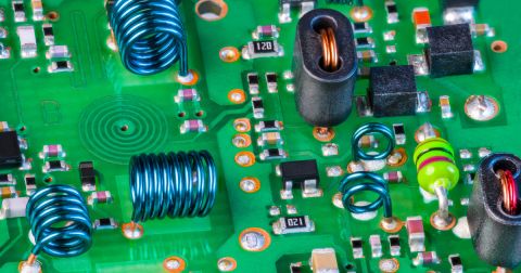
If cable entries/exits are found to carry excessive conducted emissions, even in the case where routing and layout are optimal, try to investigate before adding a common-mode choke or filter circuit. The problem could be coupling through a floating ground or the enclosure. However, in some cases, common-mode chokes are simple components that will help ensure conducted emissions compliance, and this is an easy fix if the noise problem does not hamper functionality.
Common EMC Problems Start at the Stackup
Some of the most common radiated emissions problems arise due to bad stackups. This could be because the stackup fails to suppress noise in components, or it causes bad routing practices that also lead to excessive radiated emissions. Conducted emissions failures can also result from bad stackups, which is primarily related to system-level grounding creating excessive common-mode noise.
An example stackup design strategy that helps ensure low noise, maintains impedance for high-speed/RF signals, and reduces inductive/capacitive coupling is shown below. Within a stackup, one of the simplest methods to solve certain EMI problems is to take advantage of ground. Using ground between signal layers provides shielding between signal groups while also reducing unintentional radiated emissions from signal lines. It also eases the task of maintaining return paths on signal transitions.

This strategy of maintaining system ground solves many of the simple EMI problems associated with signal propagation. While the word “simple” might imply “unlikely to cause EMC compliance failure”, this is not the case; expensive testing failures can be traced back to something as simple as layer arrangement in the PCB stackup.
A Modular Approach for Wireless
It is possible to go to market with a product that is totally modular, but only if the modules you use to build the product have individually passed EMC testing. The FCC offers Modular Certification, which allows pre-certified wireless modules to be used in a product. This will eliminate the RF testing portion of your device’s certification process as the modules will have already been certified to operate only in their intended radio bands.
This certification does not eliminate the requirement to have other emissions tests performed for your product. However, it does reduce the risk of failures and helps speed up time to market. There are other reasons to avoid these modules, such as hitting specific form factor targets and the possibility of being unable to clone or customize the design.

Should Shielding Be Used?
In my opinion, if you do things in the PCB layout correctly, then additional board-level or enclosure-level shielding should not be needed to simply pass EMC testing. The simple reason for this is that it increases component and assembly costs. For a prototype, this is most likely a negligible cost, but at high volume, these costs add up quickly. Therefore, simply from a device simplicity and cost standpoint, shielding should be avoided if possible in favor of perfecting the design and layout.
There are of course exceptions, and in some instances where a device needs to be deployed quickly, adding shielding to an existing design can be the lowest cost and lowest risk path forward. Sometimes the perfect layout just has noisy components (e.g., motors), and even with perfect circuit and board designs there is too much noise coming from the device. Some of the fastest ways to get a prototype across the finish line of EMC testing include:
- Component-level shielding, e.g., SMD or through-hole shielding cans
- Board-level shielding, e.g., edge plating
- Enclosure-mount ferrite plates
- Absorbing elastomers, compounds, and gaskets
- Metallic gaskets for large enclosures and cabinets
- Metalized enclosures
- Metallic tapes that seal mating surfaces
- Use of absorbing conformal coatings
Shielding may be a tempting option for fixing troublesome EMI problems, but if you follow the design guidelines listed above then you may find that additional shielding components and materials are not needed.

EMC Regulations
No guide on EMI and EMC compliance would be complete without a brief discussion of EMC regulations. The USA, UK, and Europe have their own sets of regulations governing EMI generation and EMC requirements in electronic equipment. These regulations are similar to each other in terms of their noise limitations, and certain products that will be sold in these various markets must comply with the prevailing EMC regulations. The list of EMC compliance requirements can be quite long, so I’ll leave that content for another article.
It is my view that designers should be aware of the regulatory standards and design practices that drive EMC compliance for several reasons. First, if you run a service bureau, this makes you much more valuable to your clients. You will have skills needed to help them navigate the regulatory hurdles that are present in a go-to-market roadmap. The other reason is that it allows you to interface more deeply with EMC test engineers and speak to them on a common level.
Now that you’ve learned about the common challenges in EMC compliance, make sure you use the complete set of PCB design tools in Altium Develop to design your PCB. Altium Designer, included in Altium Develop, is the industry’s leading CAD platform that also provides integration with cutting-edge applications for SI, PI, and EMI/EMC simulations. When you’ve finished your design, and you want to release files to your manufacturer, Altium Develop makes it easy to collaborate and share your projects.
Whether you need to build reliable power electronics or advanced digital systems, Altium Develop unites every discipline into one collaborative force. Free from silos. Free from limits. It’s where engineers, designers, and innovators work as one to create without constraints. Experience Altium Develop today!

About Author
Related Resources
Related Technical Documentation
Table of Contents
Design to Release, Without the Friction
- Keep reviews tied to the right version
- Reduce handoff confusion and rework
- Spot sourcing and release risk earlier
- Work solo, share when needed
Get Started
Thank you, you are now subscribed to updates.

