PCB Impedance Calculation and Cross Section Features in PCB Layout

When I first started laying out printed circuit boards, there wasn’t a lot of concern about controlled impedance routing. At that time, most everything was low speed and we were using larger traces and thru-hole vias for the simple four layer boards. That all changes once a board grows in speed, and changes demanded that we become more involved with the layer stackup design and specifying trace widths. At first we relied on board constraint information from different sources and personnel that we worked with, and eventually, we started using impedance calculators ourselves to set up our board stacks and design rules.
Fortunately, the next step in CAD tools is now here, and it is a pleasure to work with. Instead of doing the impedance calculations ourselves and manually copying trace dimensions into the design rules, the calculators are embedded within the PCB design tools and their information is passed directly into the design rules. Altium Designer® is a great example of a PCB layout application where this information is fed directly into the design rules from the layer stack. If this sounds like something that would be helpful to your workflow, read on and I’ll show you how it works.
PCB Impedance Calculation Methods
There are a few basic PCB impedance calculation methods that every designer should know. If you look around Altium's PCB Design Blog, there are several articles about this topic, and each seems to highlight a range of possible PCB impedance calculation options. Here are the three primary PCB impedance calculation methods:
- Using equations: Take a look at Brian C. Wadell's Transmission Line Design Handbook for a huge list of impedance equations for different transmission line geometries. There are many online calculators that will use Wadell's equations or the IPC equations for PCB impedance calculations.
- Using measurements: There are various ways to calculate the impedance of a transmission line from measurements. You can develop an empirical equation from data, or you can use an empirical equation from the IPC standards. Using time-domain reflectometry (TDR) data with a reference impedance is one method.
- Using a field solver: This uses a numerical technique like FDTD or FDFD to determine impedance. These tools are adaptable to any geometry in 2D or 3D, but they take longer to run than a simple calculator.
Altium Designer's integrated field solver was provided by Simberian, and it gives every designer an easy way to calculate the impedance of microstrips and striplines. This field solver performs impedance calculations using the 2D cross-section of your traces, giving you an accurate trace width for a given dielectric constant, copper weight, and distance from the reference plane. To get started, you need to create a layer stackup in Altium Designer and select a dielectric.
Creating the PCB Layer Stack
Altium Designer has been built to do its impedance calculations automatically. You don’t have to start the calculator from a menu or engage it somehow. It takes its information from the board layer stackup, performs the calculations, and then feeds the results directly to the design rules. This saves you a lot of time and effort in searching for an online calculator to use or finding one that you can run as an app on your phone, and then manually entering the data and retrieving the results.
In order for Altium Designer to correctly calculate the impedance, you must first make sure that it has the necessary data to work with. To do this you will work with the layer stack manager to configure the circuit board layer stack and input the board material widths (both copper and dielectric) as well as the dielectric constant. The impedance calculator will then use this information along with the target impedance values to make its trace width calculations.
To configure the board layers and input the material widths, go to the “Design” pulldown menu and click on “Layer Stack Manager”. You can build your own board layer stack or you can choose to work with one of the layer templates available in the “Presets” button. Below is a picture of a 10-layer PCB stackup.

Setting up your layers for a PCB impedance calculation in Altium Designer
As you can see above, the layer stack manager gives you the ability to change the following board layer attributes:
- Layer Name
- Type
- Material
- Thickness
- Dielectric Material
- Dielectric Constant
The layer stack manager also gives you control over many other functions such as adding and deleting layers, defining drill pairs and vias, setting up flex regions for a rigid-flex board, and backdrilling. Once you've got your board set up, you can click on the Impedance tab to start your PCB impedance calculation for different layers.
Working with the Tools to Change the Impedance Calculations
Altium Designer will base its impedance calculations on the configuration of the layers in your design. These calculations use an integrated field solver, which also accounts for copper foil roughness effects and copper etching during manufacturing. This field solver also accounts for dispersion using a wideband Debye model; a designer only needs to specify a base dielectric constant at a specific frequency and the field solver does the rest. You don't need to have formulas memorized to get an accurate PCB impedance calculation thanks to these tools in Altium Designer.
To access the PCB impedance calculation tool, just click on the Impedance tab at the bottom of the Layer Stack Manager window, and bring up the Properties panel. In this example, I've targeted an impedance of 40 Ohms for microstrip lines (top and bottom layer only). The field solver automatically calculates the width needed to produce the desired impedance while accounting for etching, copper roughness, and dispersion.

Altium s formula for stripline trace width calculations
Note that this has been specified for a single-ended trace, but we can also create an impedance profile for differential pairs. These two objectives can be satisfied simultaneously; you can specify a target impedance for single-ended traces, then you can specify a differential impedance for the same layers with the same single-ended impedance. Once you've created your impedance profiles, it's time to set them in the design rules before you start routing your PCB.
Using an Impedance Profile in the Design Rules
After the integrated field solver runs a PCB impedance calculation and creates an impedance profile, you need to go into the design rules and assign your new profile to nets in your design. To do that you need to close the Layer Stack Manager, then go to the “Design” pulldown menu and select “Rules”. Scroll down the list of rules and click on the “Width” rule as shown in the picture below. After you create a new design rule, you can select the "Use Impedance Profile" option and select the new profile you created in the Layer Stack Manager.

Setting the PCB impedance calculation routing width in Altium Designer’s design rules
In the rule shown above, the preferred width and min width have been set to the value defined in the impedance profile. However, the max width is still adjustable. Currently, the maximum width is set to 10 mil, but I normally set this to 5% higher than the preferred width. The routing tools in Altium Designer do an excellent job of sticking to the preferred width as you route your PCB.
We've also set this rule to apply to all nets. However, some nets may not need to have this design rule as they may need to have a different impedance, or they may not need to have any impedance control at all. In this case, the easiest way to assign an impedance profile to a specific group of nets is to create a Net Class with the desired nets. Note that you can create single-ended or differential pair net classes.
Once you've created a net class, you can assign the rule to one or more Net Classes in the PCB Rules and Constraints Editor. If one rule needs to be assigned to multiple nets, the easiest way to setup the design rule is to use a custom query. In the example below, I've set up a custom query that will apply my single-ended impedance profile to multiple nets. This is shown below, where the custom query applies my new PCB impedance calculation design rule to the Net Classes labeled "HiSpeed_Nets" and "NetGroup2".

Trace impedance profile applied on specific net classes using Altium Designer's width rule
Note that all the information that will be used for routing gets pulled directly from your impedance profile. The only exception is the max width constraint, which you can set in the design rule once it's created. This gives you a simple way to set routing constraints onto multiple nets with a single design rule. The same type of query functionality can be used in other design rules.
Note that, if you change the layer thickness in the PCB stackup, then the trace width required to reach your target impedance will also change. The new required trace width will be automatically imported into the design rules, but you should still go back into the PCB Rules and Constraints Editor to make sure you haven't set the maximum width value too large or too small. Once you start routing, the required width will be automatically used by the router.
Impedance Profiles For Differential Pairs
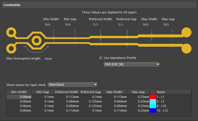
The impedance profiles created in the layer stack manager can be created for differential pairs, and then assigned to differential pairs to enforce constant width and spacing throughout the length of the route. The constraint is first setup by creating a differential impedance profile in the Layer Stack Manager, then applying this in the PCB Design Rules and Constraints Editor. The rule for differential pairs is applied in the Routing -> Differential Pairs Routing section of the PCB Design Rules and Constraints Editor. You will need to select a "Use Impedance Profile" box, just as was the case above for single-ended traces.

The differential impedance profile sets the width and spacing of traces in a differential pair
The next question that is not so obvious to answer is: what values should you use to define your differential impedance? If you are routing only on a PCB and you are not routing on layers with thick dielectrics (approximating a 2-layer board), then you can use wider spacing in the differential pairs. This is very useful for ensuring minimal mode conversion on long routes, but it is not so good for reducing differential crosstalk. Selecting tight versus loose coupling is an engineering decision just like many others, so consider the routing options carefully whenever your channel bandwidth requirement is above ~1 GHz.
Only Altium Designer gives you the most powerful set of PCB design tools to help you run a PCB impedance calculation and quickly route your board. Altium Designer is advanced PCB design software that has been created specifically to help you with your controlled impedance routing and all other aspects of designing your printed circuit boards. To find out more how Altium Designer can help you today, talk to an expert at Altium.


