Differential Pair Impedance: Using a Calculator to Design Your PCB


Differential impedance in your PCB is a bit of a complex topic that is often misunderstood. I too used to have some misconceptions about what was needed to ensure differential pairs operated correctly for different signal edge rates and high speed digital protocols. Unless your digital design is only running with single-ended buses that do not have an impedance specification (SPI, I2C, etc.), you will have to use differential pair routing to move high speed data between components. This could involve wide parallel buses like DDR, SerDes channels, or purely differential serial protocols. All of these need a precise calculation of trace impedance, including differential impedance.
The results from a differential pair impedance calculator are often misunderstood, with several definitions revolving around single-ended impedance, characteristic impedance, and odd-mode impedance being confused and sometimes used interchangeably. To help designers who might be looking for guidance, Altium created this guide to help designers understand results from a differential pair impedance calculator and some important guidelines to help implement the results into the design process.
Using a Differential Pair Impedance Calculator
It's easy to get a number out of an impedance calculator, but understanding what the number means and how to use it are the real challenges. Differential pair impedance calculators will return at least two important values, and it's important to understand what these values mean/how to use them. The differential impedance value that is returned from most calculators is equal to the sum of the odd-mode impedances for each trace:

When the two traces are designed with the exact same impedance, then taking the differential impedance and dividing by 2 gives you the odd-mode impedance value of each trace:

All of this includes contributions from coupling. In effect, the role of a differential pair impedance calculator is to calculate one of the odd-mode or differential impedances, and then use this to calculate the other while assuming the two ends of the pair obey specific geometries. Just to give designers a starting point, take a look at these differential impedance calculators you can use to get an initial estimate of the differential impedance for microstrips and striplines.
- Use an online differential microstrip impedance calculator
- Use an online differential stripline impedance calculator
Calculating Differential vs. Single-Ended Impedance
The trace impedance (single-ended) in an individual trace is normally calculated by ignoring any neighboring traces, so no coupling to other conductors in the design will be included. This means the single-ended impedance is just the characteristic impedance. This is not the case for the differential impedance; in differential pairs, the differential impedance is determined by capacitive and inductive coupling between each trace in the pair. As a result, the single-ended impedance of a trace in a differential pair is not the characteristic impedance of the same trace; the value is the odd-mode impedance and the difference arises due to parasitic coupling between the two traces. The odd-mode impedance and characteristic impedance only converge to each other when the separation between traces tends to infinity.
Coupling in differential microstrips, which determines the odd-mode and differential impedance values.
For differential pair impedance, there are some simple formulas you can use to estimate the impedance of the pair (when it is not connected to any load) using only the characteristic impedance and coupling strength. Take a look at this webinar with Ben Jordan to learn more about this calculation and to see a simple formula for differential microstrips. The calculators shown above both use the more accurate Wadell's equations for coupled transmission lines, which are widely regarded as the best analytical models that can account for lossless impedance.
For the mathematicians out there, the frequency content in a digital signal can be represented as a sum of analog frequencies, and each analog portion of a digital signal will see slightly different dielectric constant due to chromatic dispersion in the dielectric. This means that coupling in a differential pair that carries digital signals varies throughout the frequency spectrum of a digital signal or a wideband analog signal. Unfortunately, differential impedance calculators fall short in this particular area, as well as several others, which I'll explain below.
What a Differential Pair Impedance Calculator Misses
The differential pair impedance calculators you'll find online provide a good first estimate of the impedance you can expect for your particular geometry. For less than Gbps digital bit streams (usually longer than 100 ps rise time), the results will be reasonably accurate; signals in this range can have generous skew limits, so minor inaccuracies in the impedance calculation will not ruin signals as long as length matching is enforced along an interconnect. Higher data rates/faster edge rates are more prone to failure due to errors that are inherent in using simple calculator applications and an online calculator. It's important to know what a differential impedance calculator won't tell you, as well as what you need to account when designing your PCB stackup:
Propagation Constant and Losses
Most online calculators won't give you the propagation constant or attenuation value of signals being carried by a differential pair. If they do, it's only at a single frequency that is specified by the user, and this specified frequency is not being used directly in the calculation. Because digital signals are wideband and do not have power clustered at a single frequency, the result will not be representative of the real propagation behavior in your particular design. If you do get a value for the propagation constant in a differential pair impedance calculator, it's almost always just the phase velocity with no losses included. This is related to another drawback of simpler impedance calculators: the dielectric constant.
Dielectric Constant and Dispersion
For digital signals and wideband analog signals, we need to take the frequency spectrum of the signal into account when calculating differential impedance. Getting an accurate result from a differential impedance calculator requires you to know the complex dielectric constant of the substrate at all frequencies up to some limiting bandwidth value, i.e., accounting for dispersion. For a single-ended trace operating at one frequency (e.g., RF signals), it's okay if you only know the value of the dielectric constant at a single frequency. For digital signals, not taking a wideband approach and comparing propagation across the entire signal bandwidth masks the true potential for distortion and losses during propagation, as well as deviation from target impedance due to losses.

This is one reason you should leverage your fabricator's experience and material set when designing the stackup and determining impedance. They can give you dielectric constant data and a trace arrangement that hits a particular impedance. You can then program this into your design tool and use it to ensure you're within length matching limits. You can also play with the geometric parameters to make sure you're within the desired impedance window up to some tolerance.
Fiber Weave and Skin Effect
I've never seen an online impedance calculator that can account for fiber weave effects or roughness. On reason for this is the pseudo-random nature of the fiber weave. If you're not routing on tight weaves, then the skew created on each trace by an open weave is unpredictable, so you would have to approach the problem statistically. With roughness, the impedance and loss created by the skin effect and roughness is process-specific and needs to be include based on tabulated data. However, there are some basic models that can be used to determine the increased magnitude of skin effect impedance due to copper roughness, and these will be included in more advanced calculators that you won't usually find online.
Input Impedance
The values you get from an online differential pair impedance calculator corresponds to an isolated differential pair, they do not consider the load component and they are not calculating the input impedance. For complex impedance matching, the input impedance is important as this is the impedance seen by a signal as it enters the differential pair. This will need to be calculated by hand or by using a reflection simulator built into advanced routing tools, and this has to be done with the complex impedance value that includes the full dielectric constant.
Differential Pair Impedance Calculations in Your Layer Stack Designer
Because of the above limitations with simple differential pair impedance calculator tools, ECAD/EDA software companies have taken many steps to help designers speed up differential pair impedance and propagation constant calculations Your layer stack design tool should help you design to the impedance you need by giving you access to a more advanced differential pair impedance calculator. The differential impedance you get from a typical calculator you'll find online is just an approximation; more advanced tools are needed to verify the result and set a design rule that enforces the correct trace width during routing.
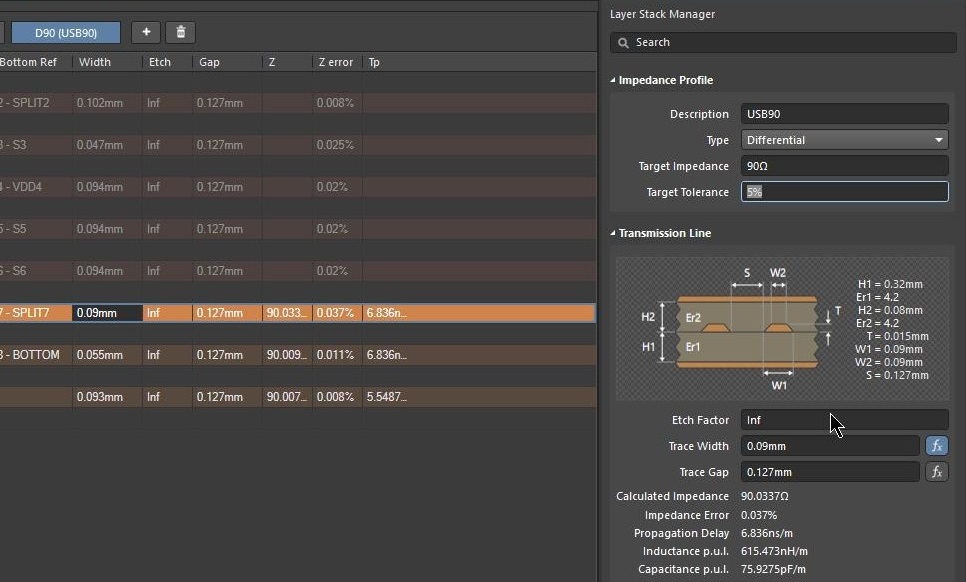
Altium's layer stackup design tool is integrated into the PCB Editor, so you can quickly access a powerful 2D field solver that accommodates the four common differential trace arrangements, including coplanar arrangements. To access these features, simply open your layer stackup in the PCB Editor and click on the Impedance tab. From here you can create an impedance profile that will run impedance calculations based on your stackup and selected trace arrangement. Make sure you copy the appropriate dielectric constant into the stackup to ensure you've calculated the correct differential impedance.

Also note that half the differential impedance, which is the odd-mode impedance of a single trace, is not the same thing as the characteristic impedance of one trace in the pair. If you plan to route your differential pairs far from each other, then the relevant impedance is the trace characteristic impedance, not the odd-mode impedance of a single trace. I've discussed this point in other articles about differential pair design and routing; you can read more in these articles:
- How to Design to a Differential Impedance Specification
- Should You Use Tight vs. Loose Differential Pair Spacing and Coupling?
Take some time to check out the Layer Stack Manager in Altium and see how you can easily use the best differential pair impedance calculator to build your layer stack. When you’ve finished your layer stack and you're ready to have your design evaluated by your manufacturer, you can release design files with Altium. No other combination of design tools makes it so easy to collaborate and share your projects.


