


PCB Polygon Management: Pour and Copper Features in Complex Layouts

At a Glance
PCB polygon pour and copper features in your PCB layout need to be carefully managed, especially when collaborating with other designers.


One PCB design tool that is critical for any PCB layout is a polygon pour feature. This useful tool can be used to quickly fill in a layout with copper to provide a customized plane shape. The rules-driven design engine in Altium Designer® also ensures that any PCB polygon pour you place in your PCB layout will comply with clearance rules and will be checked against other electrical design rules.
Layouts for complex electrical systems may need to make extensive use of copper pour to provide ground nets, power nets, shielding, and other copper structures for power and signal integrity. Backplanes, motherboards, RF products, and many other complex layouts will make use of copper pour and polygons that can’t be easily placed as custom components. Although most PCB layout software has features for placing polygons, either as components or copper pour regions, managing a range of polygons as part of a team is difficult with other programs.
When you use Altium 365®, you can easily collaborate on complex PCB design projects with a group of designers. If you’re designing a complex layout and you need to manage polygon pour, copper regions, cutouts, and other layout features, Altium 365 makes it easy to share and access the data your team needs. Here’s how the cloud-supported PCB design in Altium 365 can help your team work through a complex layout.
Tools for Managing Your PCB Polygon Pour and Copper Regions
Altium Designer already gives you access to all the information on polygon pour in your PCB with the Polygon Manager dialog. This tool gives you a simple way to see all the information about your polygons, including pour order, layer arrangement, locked attribute, and the ability to create new design rules for polygons. You can also use the selection filter in the Properties panel to access each element graphically as you work through your PCB layout.
When working with a team on a complex layout, you’ll often need to juggle multiple polygons, cutouts, or copper regions. There are some basic polygon and copper management tasks that can be difficult when working with collaborators:
- Changes to shape. This is probably the most common change that needs to be made to PCB polygon pour.
- Calling out layer and net name changes. This is a basic layout task, but complex layouts with multiple polygon/copper regions often require nets, polygons, or copper to be moved between board layers.
- Changes to net names. Polygons aren’t assigned to nets in the same way as traces. You’ll need to assign and change a polygon’s net name manually in the Properties panel.
- Changing from polygon to copper region/cutout. Polygons can be assigned to a specific net, but a copper region can overlap with all nets it touches. If you haven’t enabled online DRC for your copper regions, you may not notice that you’ve created an unintended short. Sometimes you’ll need to replace a polygon with a region object, or vice versa.
- Changes to pour order and clearances. Placing and pouring polygons is convenient with modern CAD tools, and overlap between polygons can be prevented by setting the right pour order and clearances. While working on a layout or during design review, clearances between objects may need to be adjusted, including polygons.
Executing these changes is easy with the CAD features in Altium Designer, and keeping required changes organized can be just as easy when you can see required changes directly in a PCB layout.
Use Commenting to Callout Changes and Stay Organized
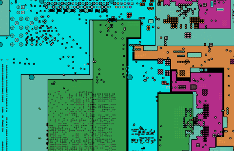
The commenting features in Altium 365 are my preferred tool for calling out changes in polygons, routing, copper regions, or cutouts. Most designers are probably familiar with placing comments on components in the Schematic Editor or PCB Editor, but you can also use the area or point comment features to callout specific changes to PCB polygon pour, cutouts, or copper regions. The image below shows what designers will see when they open up a layout with comments in Altium Designer. Clicking on one of the entries in the Comments panel will snap directly to that object in the PCB layout.

Once changes are made or responses are entered, they’ll appear in the latest version of the layout once your team member opens it in Altium Designer. This back-and-forth collaboration process between Altium Designer and Altium 365 helps designers track changes to polygon pour in a complicated PCB layout. Once changes are executed, they’ll be entered into version control so that designers can roll back to earlier designs when needed.
Comments on polygon regions can also be viewed through the Altium 365 web instance, or in Concord Pro. Designers can respond to comments on polygon regions, components, and any other locations in the layout in either Altium Designer or in the Altium 365 web instance.

Once you’ve executed a layer move, net name change, shape change, or any other change, it’s always a good idea to note this in a comment. For large groups of designers, a team leader should be in charge of checking that changes were executed properly and resolving comments.
Check These Points When Moving Polygons and Regions
Team members should also follow some basic best practices for moving and modifying polygons and copper regions. There are some points I always try to check if I need to modify polygons:
- If vias need to appear on a polygon, make sure they also appear on the destination layer.
- If the destination layer contains an overlapping polygon, you can experiment with the pour order to get the right arrangement and prevent nets from overlapping.
- If you move a polygon between layers, the pour order on the destination layer can create a broken polygon that disconnects a net.
- Before you repour, make sure to check your clearances in your design rules and create clearance rules if you haven’t already.
- Check that copper regions will connect only with the pads or vias you intended. You can zoom in close to check net names when making modifications or moving copper between layers.

When you’re ready to help your remote team get the most out of PCB polygon pour and copper region management, try using the sharing, commenting, and revision tracking tools in Altium Designer and the Altium 365 platform. Design teams can create a productive design workflow for collaborative PCB design.
We have only scratched the surface of what is possible to do with Altium Designer on Altium 365. You can check the product page for a more in-depth feature description or one of the On-Demand Webinars.


About Author
Related Resources
Related Technical Documentation
Table of Contents
Design to Release, Without the Friction
- Keep reviews tied to the right version
- Reduce handoff confusion and rework
- Spot sourcing and release risk earlier
- Work solo, share when needed
Get Started
Thank you, you are now subscribed to updates.


