Custom Pad Stack

PCB design demands precision and adaptability. From thermal connections to pad shapes, every detail matters. Pads are no longer just points; they require unique, tailored solutions. Altium Designer 24 empowers you to customize pad shapes, fine-tune thermal relief, and master rounded/chamfered rectangle pads to meet manufacturing standards, conquer tight spaces, and truly elevate your design game. Dive deeper into this enhanced feature in our new manual.
Introduction
In the fast-paced world of technology development, it’s increasingly important to have precise and adaptable designs for printed circuit boards (PCBs). As frequencies and signal complexities rise, every aspect of PCB design demands careful attention; from thermal relief connections to the very shape of pads themselves.
Pads, for example, are no longer basic conductive points. They have developed into different shapes and complicated designs, often needing unique solutions made specifically for them. What’s more, the interaction between pads and polygon pours— the thermal relief connections—has moved beyond standard rules to demand tailor-made treatments.
Considering the added complexity of components and the requirement for placing them in tighter spaces, we need to think differently about the usual shapes of paste and solder masks. The capacity to freely customize these shapes allows designers to meet strict manufacturing standards, component footprints, and optimally balance solderability and protection.
With the latest additions to Altium Designer, these critical elements of PCB design are given the attention they deserve; custom pad shapes, thermal relief customization, rounded and chamfered rectangle pads, as well as custom paste/solder mask shapes all now fall within the designer’s direct control in the Pad Stack section.
Benefits of the Altium Designer Custom Pads Stack
- Less Workaround By allowing direct implementation of datasheet or process requirements into the design, makeshift solutions or later adjustments are lessened. For example, you can add paste masks directly to through-hole components, eliminating extra soldering steps.
- More Precise Engineering Detailed thermal reliefs, customizable pad geometries, and precise solder mask dimensions elevate the fabrication integrity. These features can help create more reliable PCB assemblies— which is essential for high-frequency applications.
- Better Accuracy By offering precise pad and mask shapes, success rates or production efficiency in PCB manufacturing can be improved. This is particularly important when dealing with small component footprints—where even minor inconsistencies can result in a defective board.
- Design Flexibility With detailed control over pad shapes and thermal relief connections, a wider range of assembly methods and components can be used. You can accommodate components with unique footprints or design a board that supports both SMT and through-hole automatic assembly, for example.
- Reduced Risk of Issues Maintaining control over specifications can help prevent potential fabrication issues. You can design to avoid common problems such as solder bridging, solder balling, or tombstoning.
- Enhanced Standardization By improving important characteristics of PCBs, we establish new standards for accuracy and quality during production. With these improvements, you can execute better alignment of the solder mask. As an example, this would be important for highdensity interconnect (HDI) boards.
- Added Compatibility Customizable pad shapes and dimensions increase compatibility with various components. This can be useful when using a mix of standard and non-standard components in your design.
- Streamlined Process These features simplify the design workflow, reduce workarounds, and directly incorporate requirements in the design phase. This streamlining can be particularly valuable in complex multi-layer designs.
- Cost Efficiency By limiting the amount of revisions and edits, production costs can be significantly cut down. For example, designing throughhole components for reflow soldering can save on manual soldering costs.
- Space Optimization Custom pad shapes and dimensions support a more efficient use of the available PCB surface area. This is beneficial for highdensity designs and components with small pitches, especially Ball Grid Arrays (BGAs) utilizing via-in-pad configurations.
Summary of latest features contained in Custom Pad Stack
As with many features in Altium, the Custom Pad Stack is part of a continuous process of development and improvement. Over time, individual features were progressively added to Altium Designer. Now they are combining into a complete tool, the Custom Pad Stack.
Below is a list of the latest of them, available from Altium designer 23.8. We will take a look at what they allow us to do.
- Optimized Pad Stack Panel: All layers and options are now organized into a single, compact table, permitting individualized editing for each layer or option

- Extended Custom Shapes: Custom shapes can be applied beyond just the copper layer, expanding to paste mask and solder mask layers. Each layer can be customized individually.

- Advanced Predefined Shapes: Designers have the option to set predefined constants on each layer independently.

- Offset Support on Every Layer: The introduction of offset adjustments for predefined shapes across all layers provides another layer of customization.

- Integrated Window-Shape for Paste: The capability to incorporate multiple shapes into a single pad stack allows for the creation of a window shape for paste.

- Pin-in-Paste (PIP) Technology Support: The feature extends support for the paste layer on multi-layer/through-hole pads.

- Auto-Adjusted Thermal Relief Connections: The software can now self-adjust the number of thermal reliefs in line with the pad’s design.

- Manual Thermal Relief Editing: With enhanced user control, designers can manually add, edit or delete thermal relief connection points on pads.

Custom Pads Stack Use Case
Custom pads stack have the potential to significantly improve the design and manufacturing process of PCBs. They offer a flexible solution for unique component footprints, design requirements, and manufacturing constraints. Plus, having increased control over the design parameters can allow for more efficient, cost-effective, and robust PCB production.
Custom pads stack have the potential to significantly improve the design and manufacturing process of PCBs. They offer a flexible solution for unique component footprints, design requirements, and manufacturing constraints. Plus, having increased control over the design parameters can allow for more efficient, cost-effective, and robust PCB production.
Example 1:
Making use of the QFN-24-4x4mm for this example, we will demonstrate how to modify the standard IPC library to achieve the recommended parameters of both the manufacturer and the production process. This will help to minimize problems such as soldering inaccuracies, solder balling, component misalignment, and improper heat distribution
Input parameters:
- The pin pads should be rounded on one side, with the rounded side near the thermal pad.
- Removed solder slivers smaller than 0.1mm.
- The thermal pad in a square shape chamfered in the upper left corner by 0.25mm.
- The thermal pad paste is reduced to cover 60% of the pad’s surface and divided into four sections, spaced 0.2mm apart from each other.
I. Pin pads shape modification to one-side round shape:
1. In the pre-created IPC footprint, select the pad where you want to edit the paste layer and then, in the Properties panel, scroll down to the Pad Stack region.

2. In the Pad Stack region, in the Top Layer row, select the Rounded Rectangle from the drop-down under the Shape column.

3. Now, in the Corner Radius box, enter the desired values for rounding—where 100% represents a radius equal to the shorter pad side when selecting a single corner or two opposite corners, and half of the shorter pad side when selecting two adjacent corners.
Now, in the Corner Radius box, enter the desired values for rounding—where 100% represents a radius equal to the shorter pad side when selecting a single corner or two opposite corners, and half of the shorter pad side when selecting two adjacent corners.

II. Removing solder slivers smaller than 0.1mm:

NOTE: In this case, with a spacing of 0.15mm between pin pads, it is necessary to completely fill the gaps between the solder mask of the pin pads
1. Select all pin pads and—in the Pad Stack region—in the Top Solder Mask row, select the Custom Shape from the drop-down under the Shape column.

2. Then, switch to the Solder Mask layer and add a squareshaped fill or region to eliminate spaces between the closest pads in one of them.
Command: Right-Click Button > Place > Fill.

3. Adjust the size of the fill or region to the desired dimension.

4. Next, select the added element along with the pad and merge both of them together.
Command: Right-Click Button > Part Actions > Add Selected Custom Masks to Pad

5. Repeat the same for all other pin pads except for the outermost ones in each row.

Note that now, the modified solder mask is not a separate fill/region overlaid on the copper layer but an integrated part of the pad’s structure.
III. Thermal pad in a square shape chamfered in the upper left corner by 0.25mm:
1. Select the thermal pad and in the Pad Stack region, then, in the Top Layer row, select the Chamfered Rectangle from the dropdown under the Shape column.

2. Expand the ▶ Top Layer category, and in the Corner Radius box as you enter the desired values for chamfering—where 100% represents a chamfer equal to the shorter pad side when selecting a single corner or two opposite corners, and half of the shorter pad side when selecting two adjacent corners.
Then, after checking the Select Corners option, we can uncheck the corners where we do not want to apply the rounding. In this case, we keep only one corner checked and enter a value of 10% to achieve a 0.25mm chamfer.

IV. The thermal pad paste is reduced to cover 60% of the pad’s surface and divided into four sections, spaced 0.2mm apart from each other:
1. Select the thermal pad and in the Pad Stack region, in the Top Paste row in the Percentage % box, set a value of -40% to know the size of paste equal to 60% coverage.

2. Now, knowing the margin value of -0.317mm, you can create four pads sized at 1/4 of the large pad and space them apart by a significant value, which in this case will be 0.2mm.

3. Now, select the paste pads and the thermal pad, and merge them together. Command: Right-Click Button > Part Actions > Add Selected Custom Masks to Pad

Note that now, the modified paste layer is not a separate fill/region overlaid on the copper layer but an integrated part of the pad’s structure.
Example 2:
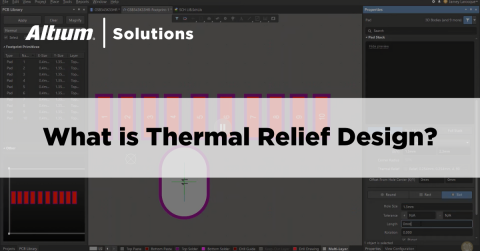
Heat can be a big problem when you’re designing circuit boards. Now, Altium lets you customize thermal relief settings to better control how your board deals with heat. Let’s look at how to do this.
1. After selecting the pad, we proceed to the Pad Stack window. Then on the signal layer where we want to make changes, we check the Thermal Relief checkbox

2. Now after clicking the Relief setting, we can open the Edit Polygon Connect Style window.

3. In addition to the already known options such as 2, 4 Conductors, a new Auto mode has been added, where a conductor will be placed on each side of the pad/ via, taking into account the minimum distance set between conductors.

4. Another addition is the ability to manually edit thermal reliefs; you can add new ones, edit, or delete selected connections. To do this, you need to right-click on the pad and choose the Pad Action option, then select the action you want to perform. After selecting the suitable option, you can easily make changes to the connections.

Conclusions
Custom Pads Stack in Altium Designer provide a higher degree of control in PCB design, enabling a tailored approach to unique component footprints and effectively reducing the need for workarounds.
The ability to independently define paste and solder mask shapes enhances PCB production by reducing defects and ensuring proper component alignment. This results in more reliable production processes and improved device performance, thanks to optimal soldering and enhanced functionality and durability of the final product.
The newly introduced functionalities for thermal reliefs offer designers greater flexibility and control. Whether it’s adding, editing, or deleting specific connections, these custom options make it easier to meet the unique requirements of any PCB design project. Overall, it’s a significant step toward a more customized and efficient design process.
With Сustom Pads Stack, designers have greater creative freedom, allowing them to not just meet, but exceed datasheet/ process requirements. They could devise tighter tolerances or denser designs, thus enhancing PCB performance beyond traditional standards, fostering innovation in electronic design.
Altium Designer continues to grow, with the development of custom pads stack emphasizing its commitment to empowering users with advanced, precision-based tools for electronics design. This reinforces its position as a leading software choice for professionals in the electronics industry.

