









Move Interference Checking to ECAD For a More Efficient Flow

At a Glance
The completed electronic design moves to mechanical designers for interference checking for electronic design. That iterative approach delays and can even cause missed deadlines.


Electronic product development involves mechanical and electrical assemblies that must coexist within a constrained physical envelope. Getting that fit right is not optional: a connector that protrudes past the enclosure wall, a tall capacitor that contacts the chassis, or a mounting hole that lands on a trace are all problems that block manufacturing. The traditional approach to solving these problems pushes interference verification downstream, into the mechanical designer's domain, after the PCB layout is already complete. That handoff sequence is where schedule risk accumulates.
When the ECAD tool cannot import enclosure geometry or accurate 3D component bodies, the electrical designer has no practical way to verify clearances. That verification responsibility defaults entirely to the mechanical team, who receive the completed assembly, identify violations, and relay correction requirements back to the electrical designer. The other option for MCAD-deficient ECAD software is to export mechanical files from the ECAD environment, and re-import these into MCAD to reconstruct the PCB assembly model in MCAD software.
Each cycle through this loop costs time. In programs with tight schedules or concurrent engineering dependencies, multiple back-and-forth iterations can push tape-out and prototype build dates by weeks.
How do you shorten this timetable? You need a methodology that gives electrical designers the opportunity to verify interference before the design is handed off to mechanical designers. Using that methodology can reduce iterations, save time, and improve the overall accuracy of your schedule. Let’s look at how that methodology works.
Don't Stretch Your Schedule With Late Interference Checks
A single ECAD-to-MCAD handoff with interference violations is manageable. The problem compounds when the violations trigger component repositioning, which then invalidates routing, which requires re-review of signal integrity constraints, which may require another stackup or footprint change. A connector that needs to shift 2mm to clear a boss feature can cascade into differential pair re-routing, length matching corrections, and updated fab notes. None of that work adds design value; it repairs a problem that existed before the first handoff but was not visible to the engineer doing the layout.
The schedule impact is always difficult to recover, and no one likes re-working a PCB layout just to accommodate mechanical changes that should have been obvious. Mechanical designers working concurrently on enclosure tooling or structural analysis cannot finalize their work while waiting for a stable board outline and component height profile. Every iteration that returns an unresolved interference violation holds the entire mechanical program in place.
Shift Verification Left With STEP Integration
The methodology that eliminates most of this iteration is straightforward: bring the 3D geometry into the ECAD environment before the design leaves the electrical team. This requires two inputs. The first is an accurate 3D body for each component, typically a STEP file sourced from the component manufacturer or modeled to the published mechanical envelope. Embedding these models as component properties in the library entry ensures the 3D representation travels with the footprint throughout the design. The second input is a STEP export of the mechanical enclosure from the mechanical team, imported into the PCB editor as a board-level 3D body.
With both inputs present, the electrical designer can perform clearance checking within the ECAD tool against defined rules. Components that violate the clearance envelope or physically intersect the enclosure geometry are flagged in the 3D view. The designer resolves those violations by repositioning components, adjusting board outline, or coordinating a geometry change with the mechanical team before any formal handoff occurs. By the time the design reaches the mechanical team, the interference check has already been performed against the actual enclosure geometry, and the remaining review focuses on fit confirmation rather than problem discovery.
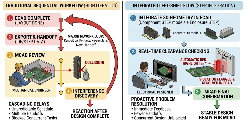
Figure 1 - File export workflow for mechanical verification versus integrated 3D interference checking in ECAD.
3D Clearance Rules and Online Checking in Altium Designer
Performing interference checking inside ECAD requires the tool to evaluate 3D body geometry against clearance constraints, not just 2D courtyard extents. Courtyard-based checking catches footprint overlaps on the board surface but does not account for component height, angled connector housings, or enclosure features that project inward from the lid. Real interference is a three-dimensional problem.
Altium Designer supports both import and export of STEP models and files, allowing electrical inference checking within the electrical design. The component clearance rule verifies that all 3D bodies and models within the design adhere to the constraints you have defined.
The online design rule checking capability within Altium Designer notifies you of collisions and highlights the collisions location in green, identifying the violating primitives. There is also an identifier when a given STEP model or 3D body violates the specified clearance. The primitives that are being assessed are the STEP files of the components and the STEP file of the mechanical housing. The image below illustrates that the connectors do not correctly fit within the enclosure, so they are highlighted.

Figure 2 - Collision and clearance violations highlighted in green
The practical requirements for this capability are:
- STEP import for individual components, embedded as component properties in the library
- STEP import for enclosure and mechanical features at the board level
- Rule-based 3D clearance checking with configurable minimum clearance values
- Online DRC that updates violation status during interactive placement
If the ECAD tool cannot satisfy all four of these, the interference checking must remain in MCAD, and the iteration problem persists. The worst case is verification in a prototype, which always creates risk of re-spinning the board, re-designing and re-building the enclosure, or both.
The next figure shows the result of changes made to the connector positioning so that the electrical assembly fits securely within the housing.

Figure 3 - The absence of any highlighting means that the assembly now fits within the enclosure
Resolving interference within ECAD does not eliminate the MCAD review entirely. Mechanical designers still need to perform structural analysis, confirm enclosure assembly tolerance stackups, validate fastener engagement lengths, and review thermal paths. The difference is that the first handoff arrives with known-good interference status. The mechanical team is no longer the first line of defense for clearance violations; they are reviewing a design that has already been checked against their geometry.
Instead of a violation-identification exercise that generates a correction list, MCAD can provide a confirmation review that either passes cleanly or surfaces issues specific to tolerance analysis or assembly sequence, which are genuinely mechanical domain problems. That is a more efficient use of the mechanical team's time, and it produces a more stable handoff state for both teams.
| Approach | Where Interference Is Found | Redesign Effort |
|---|---|---|
| ECAD-only, no 3D | MCAD review after handoff | Electrical redesign driven by mechanical feedback |
| ECAD with courtyard checking | MCAD review after handoff | Partial; courtyard misses height and 3D enclosure features |
| ECAD with STEP + 3D rule check | In ECAD before handoff | Electrical designer resolves issues in context |
MCAD CoDesigner: Full Mechanical Integration With ECAD
Altium's MCAD co-design is designed to bridge the gap between ECAD (electrical) and MCAD (mechanical) design domains, ending the days when PCB assemblies were "thrown over the wall" to mechanical engineers. It connects Altium projects to popular 3D MCAD applications, enabling multidisciplinary teams to participate in collaborative engineering while eliminating many of the manual file exchange processes normally required for enclosure design, constraint definition, and interference back-checking.
ECAD-MCAD collaboration is the process of synchronizing electrical and mechanical design data. For mechanical engineers, it means fewer surprises and less rework. Rather than relying on exported STEP, IDF, IDX, and DXF files or manual updates, it enables direct collaboration to work with native geometry within your mechanical CAD software. An electrical engineer can push design changes to the preferred MCAD software so mechanical engineers have accurate board outlines, component placement, and copper geometry. This allows each side to work on the latest changes without delays or miscommunication.
- Bi-directional Synchronization: Engineers can synchronize PCB designs between Altium Designer and popular MCAD software, ensuring both teams work on the same version of the design at all times, reducing the risk of errors and rework.
- Advanced Copper Geometry Support: Mechanical engineers get the clear electrical engineering data they need to perform detailed mechanical checks or FEA, with support for extruded copper and via transfers for copper geometry and 3D mask layers.
- Efficient CAD File Sharing: Designers use their preferred tools while the Altium workspace integration manages data and design transfer automatically, cutting development time, minimizing re-spins, and accelerating time to market.
How the Push-Pull Process Works
MCAD CoDesigner implements a simple Push-Pull process. Updates on one side can be transferred to a colleague in seconds, triggering a notification in the collaborator's co-design panel, and each side can keep track of changes by adding comments to each Push operation. This instant exchange of critical data is accomplished without the need for manual IDF/IDX/STEP/DXF file imports and exports.
The push-pull functionality makes an Altium project accessible to a mechanical engineer from within Altium Designer. Once the design is imported into an MCAD application, any changes made in the MCAD tool are synchronized back to the ECAD side. When pulled back into Altium Designer, the PCB layout data immediately updates to reflect changes in the board outline and copper.
Supported MCAD Applications
PCB designs can be imported into SolidWorks, Autodesk Inventor, Fusion 360, or PTC Creo, giving you everything needed for product development in a streamlined workflow.
For more details, you can visit:
For an overview of the MCAD CoDesigner capabilities, watch the video below.
Conclusion
Interference checking for electronic design is a necessary and critical part of the design process: quite simply, your product cannot be built if the electronic assembly does not fit in the enclosure. Passing a design back and forth between electrical and mechanical designers costs time and money. Checking clearances within the electrical design tool is a much better and more efficient option.
Moving electrical interference checking to an earlier point in the design flow requires an ECAD tool capable of importing component and enclosure STEP files and 3D rule checking. With the integrated 3D interference checks in Altium Designer, and the MCAD CoDesigner tool for collaboration with mechanical engineers, any workflow is possible in Altium Designer. The unified environment of Altium Designer gives you more efficient avenues to complete the design process. The result is a quicker design time leading to on-time product release.
Whether you need to build reliable power electronics or advanced digital systems, use Altium’s complete set of PCB design features and world-class CAD tools. Altium provides the world’s premier electronic product development platform, complete with the industry’s best PCB design tools and cross-disciplinary collaboration features for advanced design teams. Contact an expert at Altium today!

About Author
Related Resources
Related Technical Documentation
Table of Contents
Solutions for Every Role and Team
- Discover and evaluate design options earlier
- Develop in one shared workspace
- Scale with control and compliance
- Connect every stage of hardware development
Learn More
Thank you, you are now subscribed to updates.



