


Planning a Multilayer PCB Stackup

At a Glance
Multilayer PCB stackup planning with the only unified PCB design platform has benefits beyond the obvious, click to learn more.


Today’s PCBs are rarely designed on one- or two-layer boards. With the high density of connections and the number of components that are used in modern PCBs, your next design will probably be a multilayer PCB. If your next device has an odd form factor, then you will probably be using a rigid-flex PCB. No matter what type of circuit board you need to design, or whether you're designing something more advanced like UHDI or packaging, implement the right multilayer PCB stackup design process to ensure success.
This guide will focus on multilayer PCB stackup planning from multiple perspectives, such as end application and signal integrity for advanced designs. Many PCB stackup planning guides can only scratch the surface and do very little to address the needs of high-reliability, high-density packaging, or unique PCB material sets like metals and ceramics.
Start with the End Application
If you're at the stage where you're planning a multilayer PCB stackup, then you probably already know your end application and the type of board you want to use. Your application might require rigid, rigid-flex, flex or FPC ribbon, or an HDI build. If you're building something more specialized, such as UHDI or an IC substrate, you will have to start with the package type or take a substrate-like PCB approach.
Start here to understand what material sets you will need for your multilayer PCB stackup. As you move out on the density, frequency, edge rate, or thermal curves, your design will move farther away from basic FR4 with rough electrodeposited copper and will instead require more advanced materials. The table below outlines some of the material sets you will need in different types of designs.
|
Moderate-speed digital (USB, SPI, etc.) |
Standard FR4 |
|
High-speed digital (DDR,multi-G Ethernet, etc.) |
Low-Dk FR4 (Dk > 3.8) or advanced FR4 (Dk < 3.8) |
|
RF below ~10 GHz |
Low-Dk FR4 (Dk > 3.8) |
|
RF above ~10 GHz |
Advanced FR4 (Dk < 3.8) or PTFE |
|
Power electronics, high voltage/low heat |
Standard FR4 with high CTI |
|
Power electronics, high heat |
Standard FR4, metal core, or ceramics |
|
HDI, substrates or substrate-like PCB |
Standard FR4 and HDI materials |
PCB Laminate Material Properties to Consider
PCB material data sheets provide a lot of the information you will need for various applications. There are some particular values in data sheets to look at when planning a stackup:
- Dielectric constant
- Loss tangent
- Glass transition temperature
- Glass reinforcement weave style
- CTE value
- Decomposition temperature
- Breakdown voltage
- CTI value for high voltage operation
- Curing agents
- IPC slash sheet compatibility
- Thermal conductivity
- Mechanical moduli values
- Drilling process compatibility
For FR4 materials, there are a few PCB material properties that will be quite similar across various FR4-rated laminates: glass transition temperature, CTE values, mechanical moduli, and thermal conductivity. Other values can have more variance due to the resin chemistry and material construction. The values in the table below apply to more advanced or exotic materials, such as ceramics, polyimides, PTFE-based laminates, and low-loss FR4 laminates.
When you look at the more advanced spectrum of the PCB materials market, you see much larger variation in things like dielectric constant, loss tangent, and even CTE and glass transition temperature values. For example, consider PTFE-based laminate materials; these can have wide variance in Dk and Df values due to the filler materials. If certain Dk values within a specific range are needed, then a designer may need to look at advanced FR4 or PTFE materials for stackup planning.
Material Thickness
The thickness of PCB materials is most often a part of PCB stackup planning when performing a controlled dielectric or controlled impedance design. Whether the designer takes responsibility (controlled dielectric) or whether the manufacturer takes responsibility (controlled impedance), the thickness of the laminate plays a role in determining the impedance and signal integrity in the PCB.
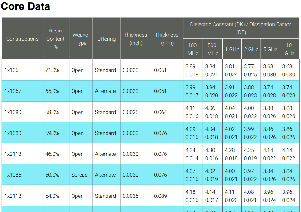
However, there are many other situations that do not involve impedance control where the material thickness is still important and is a part of stackup planning and material selection. When selecting the material, determine the availability of various material thicknesses first by consulting manufacturer data sheets or catalogs. For some materials, you may find that your desired thickness is not available. Consider the example shown below from Isola for their 370HR material platform; Isola makes these material data tables available on their website so that a designer can select an appropriate dielectric constant and thickness for their application.
Excerpt from Isola 370HR Dielectric Constant (DK)/Dissipation Factor (DF) Table
When looking at high layer count PCBs, maintaining a reasonable thickness will require selecting thinner laminates. Most FR4-grade laminates in their standard thicknesses can be used to build standard PCB stackups with up to 8 to 10 layers. Beyond that limit, board thicknesses tend to increase in order to handle the higher layer counts.
Thickness also becomes very important when HDI design techniques are needed due to the requirements for fabrication process compatibility and requirements on trace width. Process compatibility also impacts another type of stackup: a hybrid PCB stackup.
HDI and Hybrid Designs
HDI designs use thinner layers not only to reach very narrow trace widths with 50-ohm impedance but also for process compatibility with microvia fabrication. HDI designs can be constructed with mechanically drilled vias, which allow thicker layers and larger aspect ratios on via sizes. When via diameters drop below 6 mil, they must be laser-drilled, and the allowed aspect ratio on the drilled vias becomes small to ensure reliability. This is one of the major factors that limits HDI PCBs to using very thin outer layers.
The table below provides some typical aspect ratio limitations in HDI process capabilities commonly found in the U.S. Note that these process capabilities are evolving as more companies invest in UHDI fabrication with additive processing techniques.
|
Mechanical Drilling |
Laser Drilling |
|
|
Aspect ratio |
Typical values:
|
Typical values:
|
|
Drilled hole diameter |
6 mil minimum |
2-3 mil minimum |
|
Layer thickness |
Typical values:
|
Typical values:
|
Hybrid stackups are another type of design that limits material types and thicknesses. In a hybrid PCB stackup, a mixed material system is formed. This could be, for example, PTFE laminates paired with standard FR4-grade laminates, or a single HDI layer built on a standard stackup. This is typically done when only one layer requires advanced capabilities, while all other layers can be made from more common materials.
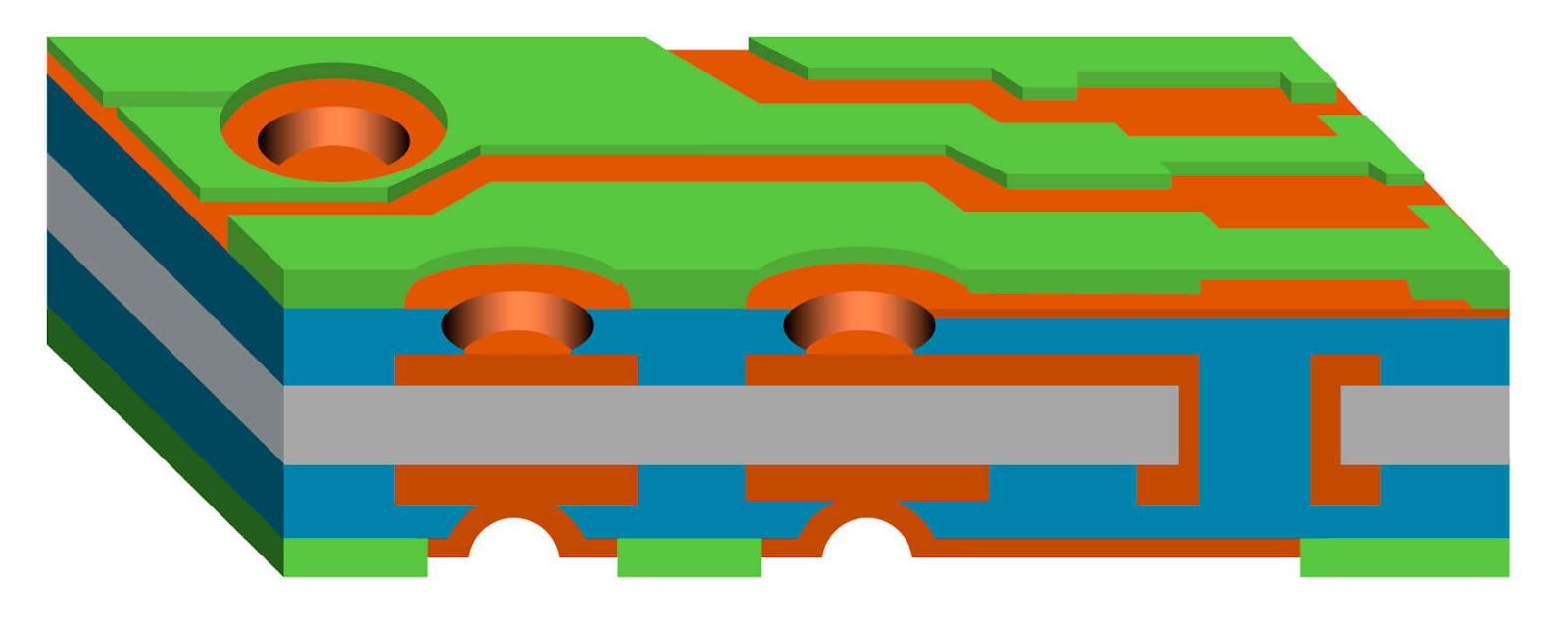
An example frequently shown from radar designs is outlined below. In this stackup, PTFE is used on the top layer while FR4 is used on all other layers. The top layer holds the RF routing and antennas, and this layer would typically use blind vias to eliminate stubs.
Example hybrid PCB stackup that mixes PTFE with standard FR4. This design could allow for blind vias on the outer layers (Type 1 HDI stackup), as well as mechanically drilled buried vias.
The same process and requirements apply in much higher density designs, such as substrate-like PCBs and designs that use chip-on-board. Substrate-like PCBs, or an equivalent integrated circuit substrate, generally require very thin layers and use integrated circuit build-up films that are laser-drillable and compatible with additive processing. The typical result for integrated circuit substrates and substrate-like PCBs is a PCB stackup with the same basic structure as standard HDI stackups. You can also have any-layer stackups with stacked blind and buried vias in these applications, just like in a standard HDI PCB stackup.
Example IC substrate stackup. Image source: KLA Tencor.
Before mixing and matching different types of PCB materials, ensure you check your material selections and stackup design with the fabrication house. They will verify that they can press the materials into a stackup and warn you of any reliability concerns. Also, inform them if you will use HDI techniques in your stackup, as this will affect the allowed layer thicknesses and layer orders used in the PCB stackup design.
Sub-Lamination Planning
When designing and planning a PCB stackup, the use of HDI techniques with microvias creates sub-lamination steps. Each sub-lamination step adds fabrication costs as it forces the drilling and pressing operations to repeat for each lamination cycle. Every HDI layer adds a new sub-lamination cycle to the stackup fabrication process. Although this is normally associated with HDI builds, it is not unique to HDI builds with laser-drilled microvias. PCBs with mechanically drilled blind and buried vias also require multiple lamination steps.
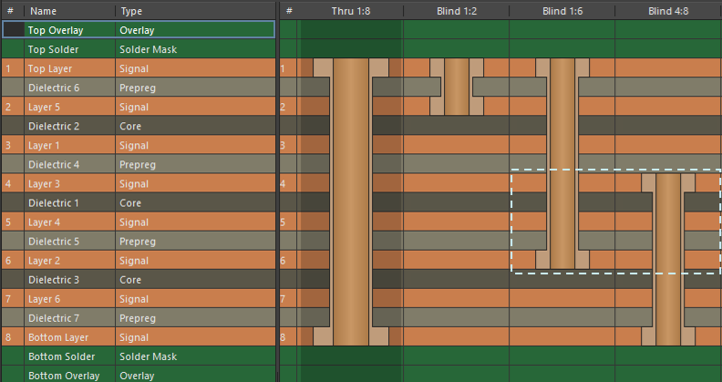
Consider the PCB stackup below, which has multiple laminations and overlapping blind/buried vias. Due to the overlapping blind and buried vias, multiple sub-lamination steps will be needed to build this PCB stackup.
These crossing blind vias require additional drilling steps that add cost and complexity to PCB stackup fabrication.
When the vias are crossing in this way, it is often unnecessary from a design standpoint and can add significantly to costs. A better plan for this stackup is to merge overlapping blind and buried vias into one larger via and allow trace connections on any intervening layers. This reduces the number of sub-laminations needed to build the PCB.
Any use of back drills is also an important part of sub-lamination planning. For example, back drills can be applied within a single lamination, and subsequent lamination cycles can be built on top or below the back-drilled lamination region. You can also back drill through multiple laminations once they are stacked.
Flex and Rigid-Flex PCB Stackup Planning
Flex and rigid-flex PCBs also require a stackup planning process, but they use different materials and layer arrangements. Flex or rigid-flex designers have additional mechanical points to include as part of a PCB stackup planning process:
- Fixation or mounting hole locations
- Bending locations and bending radii
- Whether bending is static or dynamic
- Rigid sections or stiffeners used in a flex PCB stackup or rigid-flex PCB stackup
- Unique rigid-flex stackup constructions, such as bookbinder construction
- Whether plane layers are needed for certain signals in the design
- Allowances for unique processes, such as sintered via fabrication
Flex regions in the PCB stackup use polyimide base materials for dielectric insulators separating copper layers, as well as for adhesives and coverlays. These materials are much thinner and can be used in odd numbers of layers, as well as asymmetric layer combinations without balanced copper. Although the design rules differ from standard rigid boards, flex PCBs and rigid-flex PCBs give designers significant freedom that would not be available in systems of rigid PCBs.
To learn more about the important design rules impacting flex PCBs, watch the video below.
Additional Materials: Ceramics and Metals
While less common, metal cores and ceramic cores can also be used to build PCB stackups. These designs are found in industries such as automotive, industrial systems, power electronics, and industrial-grade lighting. A typical approach is to replace one side of the PCB with a metal or ceramic slab, or to replace the inner core with one of these materials, with the primary goal being to significantly increase heat dissipation.
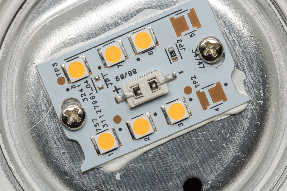
Metal-backed PCBs are common in high-power lighting systems.
If you've never designed one of these PCBs yourself, consider contacting a PCB manufacturer that supports these material systems. Not all manufacturers have the expertise to ensure high yield when using metal-back, metal-core, or ceramic-core designs. Different manufacturers may offer different capabilities and have strict PCB design rules regarding these stackups, so obtain this information first before beginning your design.
A Comprehensive Process for PCB Stack-Up Planning
A failure to plan a PCB stackup correctly is one of the most common causes of signal integrity failure, power integrity failure, or EMI failure. An experienced designer would roughly estimate that 50% of the most common problems in these three areas are solved or prevented by designing an appropriate PCB stackup. To get it right the first time, consider this simple PCB stackup planning process as part of your design workflow:
- Start by understanding your end application and the type of stackup required (rigid, flex/rigid-flex, or metal/ceramic).
- Determine your density requirements based on pin pitches or high-density components like BGAs, as this will determine required trace widths and via sizes, and may limit material options and thicknesses.
- Following Step 2, count up your signal layers based on the number of controlled impedance interfaces, number of rows in the largest BGA, and/or number of power and ground layers required.
- Set the layer thickness and trace width pairing based on Step 2, and make sure to perform this for all layers planned for controlled impedance routing.
- Check the stackup thickness against any mechanical requirements you might have, and adjust core layers appropriately.
This process is not guaranteed for every design, but it's general enough to handle high-speed PCB designs, high-density designs, unique stackups that integrate ceramics or metals, and even some flex designs. In addition, make sure you choose a PCB stackup planner that gives you full control over your material properties, dimensions, and layer counts.
Whether you need to build reliable power electronics or advanced digital systems, use the complete set of PCB design features and world-class CAD tools in Altium Designer®. To implement collaboration in today’s cross-disciplinary environment, innovative companies are using the Altium 365™ platform to easily share design data and put projects into manufacturing.
We have only scratched the surface of what’s possible with Altium Designer on Altium 365. Start your free trial of Altium Designer + Altium 365 today.

About Author
Related Resources
Related Technical Documentation
Table of Contents
Design to Release, Without the Friction
- Keep reviews tied to the right version
- Reduce handoff confusion and rework
- Spot sourcing and release risk earlier
- Work solo, share when needed
Get Started
Thank you, you are now subscribed to updates.

