Laser-Drilled Microvia-in-Pad Technology in Your HDI PCB

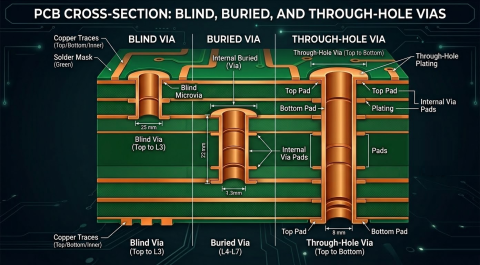
Microvias are the big enabler of HDI PCB designs with very fine pitch BGA packages. The package pitch and ball count collectively determine the number of layers needed to fan out all pins in a BGA package. With larger pitches, vias can be larger and can be placed as mechanically drilled vias, even when multiple laminations are needed. At smaller pitches, large via sizes become unusable, and a more dense microvia formation process is needed.
When you reach a high enough ball density under a BGA package, microvia placement tends to come with via-in-pad placement. The two have to go together in most cases to fit the vias underneath a package. When you find that BGA pitch values demand microvia-in-pad, follow these HDI PCB design rules to ensure reliable microvia formation.
The First Step: Contact Your HDI Fabrication House
Before you start placing microvias in your PCB layout, contact your fabrication house to get some very important information. Not all PCB fabrication houses offer HDI fabrication with laser-drilled microvias in all of the standard HDI stack-up types. For example, some fabrication companies can provide i + N + i HDI fabrication but not ELIC fabrication. The information you should obtain includes:
- Subtractive etching limits or additive deposition limits
- Laser drill depth limits
- Laser drill hole diameter limits
- Tolerances on laser drill hole locations
- Assembly and inspection capability appropriate for your BGA ball pitch
- Via-in-pad finishing options (filling options, cap and plate, planarization, etc.)
- Maximum number of stacked blind/buried microvias
- Recommended aspect ratio limit
- Laser-drillable prepreg thickness and glass weave style availability, assuming FR4 materials
- Alternatively, buildup film availability, such as Ajinomoto Build-up Film (ABF)
Some of the values in this list, for example, the aspect ratio and blind/buried via stacking limits, are available as rules of thumb. However, gathering this information before completing a design ensures you comply with specific DFM (Design for Manufacturability) requirements, especially as you decide where to manufacture and the level of compliance you require. The last thing anyone needs is to complete a design destined for manufacturing in the US, only to find that US manufacturers will no-bid the project.
HDI PCB Laser Drilling Process Limits
The PCB laser drilling process uses a tightly focused laser beam to create holes in a PCB, which are then plated to form vias. PCB laser drilling uses a CO2 or UV laser that ablates the material and leaves behind an opening for plating. The recoil pressure from fast heating by the laser beam material ejects excess molten material from the hole, so there is generally no additional cleaning step required.
There are some size limitations that must be followed when designing a PCB for laser drilling:
- Hole size: The laser beam spot size determines the hole diameter, and the exposure time determines the hole depth.
- Hole types: There is no layer limitation because these holes are used in a single lamination. Laser drilling can be used for microvias, stacked vias, and staggered vias.
- Material types: Prepregs that will be used in a laser drilling process must be laser-drillable; not all prepregs can be used with laser drilling.
A typical maximum depth for a laser-drilled microvia is 10 mil with 1:1 aspect ratio. Typical hole sizes can be as small as 2 mil. Tolerances on hole location can be much tighter than is the case with mechanical drilled holes. Also note that these specs can vary by laser drilling machinery, so check with your manufacturer for their specific aspect ratio limits, hole size limits, and hole depth limits.
Example: Determining Allowed Drill Parameters
From the design perspective, the aspect ratio limits, material availability, and clearances under a BGA all contribute to determining the allowed drill size for a set of blind and buried vias. To see how this works, we can look at a simple example with a 0.5 mm pitch BGA and a nominal land pattern size.
First, take a look at the table in this article: this table provides IPC-7351 compliance land pattern sizes for various ball sizes on the bottom side of a BGA package. If we take Texas Instruments CBC package as an example (see below), we can see that this BGA package has a ball size of 0.3 mm and a ball pitch of 0.5 mm. If we choose the nominal land pad size for the BGA footprint, we would have a pad size of 0.25 mm (nominal value), although the IPC-7351 standard allows for pad size down to 0.2 mm.
BGA pad arrangement for Texas Instruments CBC package.
Based on the 0.5 mm pitch and a pad diameter of 0.25 mm, we would have a spacing of 0.25 mm (9.8425 mils) between the edges of each pad, and 13.92 mils in the diagonal direction.
Assuming we want to comply with standard IPC product class definitions, such as Class 2 or higher, this spacing between the pad edges in the diagonal direction would not be enough space for a mechanically drilled dog-bone fanout, even down to a 6 mil drill diameter. This is because the via pad will not be large enough and will run against the limits of subtractive etch clearances. Therefore, we need to use a very small drill diameter for dog-bone fanout (which will not be possible), or we could use a larger laser drill diameter if we place the vias in-pad.
If we match the via land pad size to the solder pad size, the via could have the following geometry:
- 4 to 6 mil laser drill diameter, depending on IPC product class and producibility level
- Assuming AR = 1 (maximum), 4 to 6 mil surface dielectric thickness
- Same parameters for each stacked buried via that is drilled into the stack-up
This completes the laser-drilled microvia-in-pad design without forcing the use of smaller vias, which could violate the aspect ratio limit. Additionally, 4 to 6 mil thick laser-drillable prepreg laminates for use as HDI buildup layers are readily available.
Microvia-in-Pad Reliability
The reliability of laser-drilled microvia-in-pad structures has been investigated by IPC’s High-Density Packaging User Group (HDPUG). Specifically, the group investigated the failure rate of microvia-in-pad compared with microvia used in fanouts for various no-lead packages. They examined the following packages:
- Ceramic BGA (CBGA)
- Organic substrate BGA
- 72-pin QFN
For the specified packages, the results show a similar or lower lifetime for microvia-in-pad versus microvia in a dog-bone fanout. For the traditional BGA and QFN, lifetime decreased by only 9% and 12%, respectively, with microvia-in-pad. For the CBGA package, the lifetime was reduced by a staggering 57%. Weibull plots from the study are shown below.
Failure rate plots for a 192-pin BGA package with microvia-in-pad. The BGA without microvia-in-pad clearly has longer lifetime.
While the results do show a decrease in lifetime with microvia-in-pad, more context is needed before making additional statements regarding reliability. For example, one would expect the failure rates to depend on factors like aspect ratio, the number of stacked vias, etc.
Another study from Sanmina provides some excellent guidance on voiding in microvias, which is the critical failure mechanism arising in these structures:
Whether you need to build reliable power electronics or advanced digital systems, use the complete set of PCB design features and world-class CAD tools in Altium Designer®. To implement collaboration in today’s cross-disciplinary environment, innovative companies are using the Altium 365™ platform to easily share design data and put projects into manufacturing.
We have only scratched the surface of what’s possible with Altium Designer on Altium 365. Start your free trial of Altium Designer + Altium 365 today.


