


PCB Routing Strategies for High Layer Count Stackups


Strategies used to route PCBs with higher layer counts are diverse and will depend on the functionality in the PCB. Boards with high layer counts can involve many different types of signals, ranging from groups of slow-speed digital interfaces to multiple high-speed digital interfaces with different signal integrity requirements. This presents a challenge from the perspective of planning routing and assigning signal layers to various interfaces.
We can't mention routing strategies in high-layer-count PCBs without also mentioning pinout design in many BGAs. A high-pin-count BGA can contain many different digital interfaces, particularly if the component is a typical microprocessor or an FPGA. This is one of the most common drivers of high layer counts in the PCB.
As we have multiple challenges presenting themselves simultaneously in a high-layer-count design, I'll run over these challenges and some strategies you can use to successfully route a high-layer-count PCB.
What Drives a High PCB Layer Count?
As I mentioned in the introduction, the most common factor that will drive a PCB to have very high layer counts is the presence of a large BGA. These components have high pin counts on the bottom side of the device, and they will require more layers in order for signals to reach pins. Because these components are often specialized ASICs, microprocessors, or FPGAs, they also contain many digital interfaces with different signal integrity and routing requirements, as well as many power and ground pins.
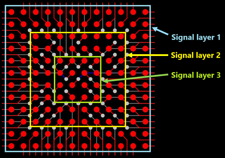
Many designers will recall the simple formula for estimating the number of layers required to reach all pins on a BGA. When the BGA pitch is large enough for a signal to be routed between pins, we can fit two rows of BGA pins per signal layer:
For a coarse-pitch BGA package where we can fit traces between balls, we can route 2 rows/columns per layer.
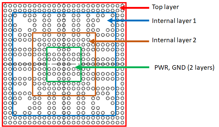
Some BGA footprints can be rather complex with missing balls in the inner rows. An example is shown below; it is likely that this BGA will not follow the same layer count calculation used for the standard BGA shown above.
Learn more in this article with Charlie Yap.
When the component has a much finer pitch and we cannot fit tracks between pads in the BGA footprint, we need to double the required layer count. When many of the pins are power and ground, the layer count will definitely decrease. It is also possible that a large number of quad packages produce the requirement of high layer counts. At the high end, these can have a couple hundred pins, certainly not the high number you would see on a moderate-size BGA.
Routing Strategy 1: No Strategy at All!
The "no strategy" strategy is by far the simplest and focuses only on minimizing layer count while ensuring solvability. It can start by selecting the required number of layers and routing out from the BGA using a standard fan-out approach, applying a fixed layer count and attempting to pack all the traces in, or routing freely and adding new signal layers as needed. It applies when:
- You are not worried about separating different impedance specifications into different layers
- All interfaces do not have an impedance specification, such as SPI
- All the interfaces have the same impedance requirement
- The number of impedance-specified interfaces is small (maybe 1 or 2)
Needless to say, routing with this strategy might not appear very organized, but the reduced focus on signal integrity in favor of solvability can help keep layer counts lower than in other strategies.
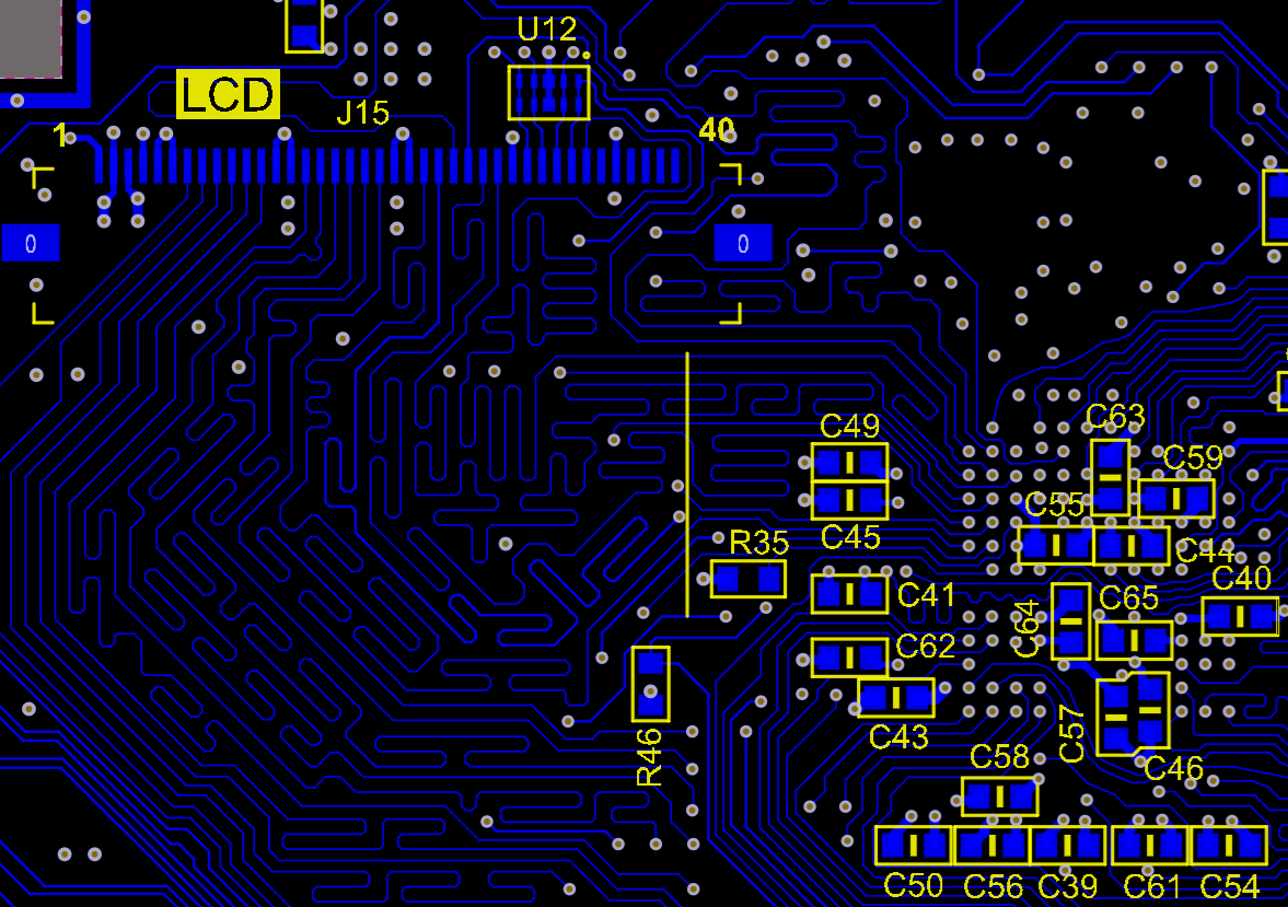
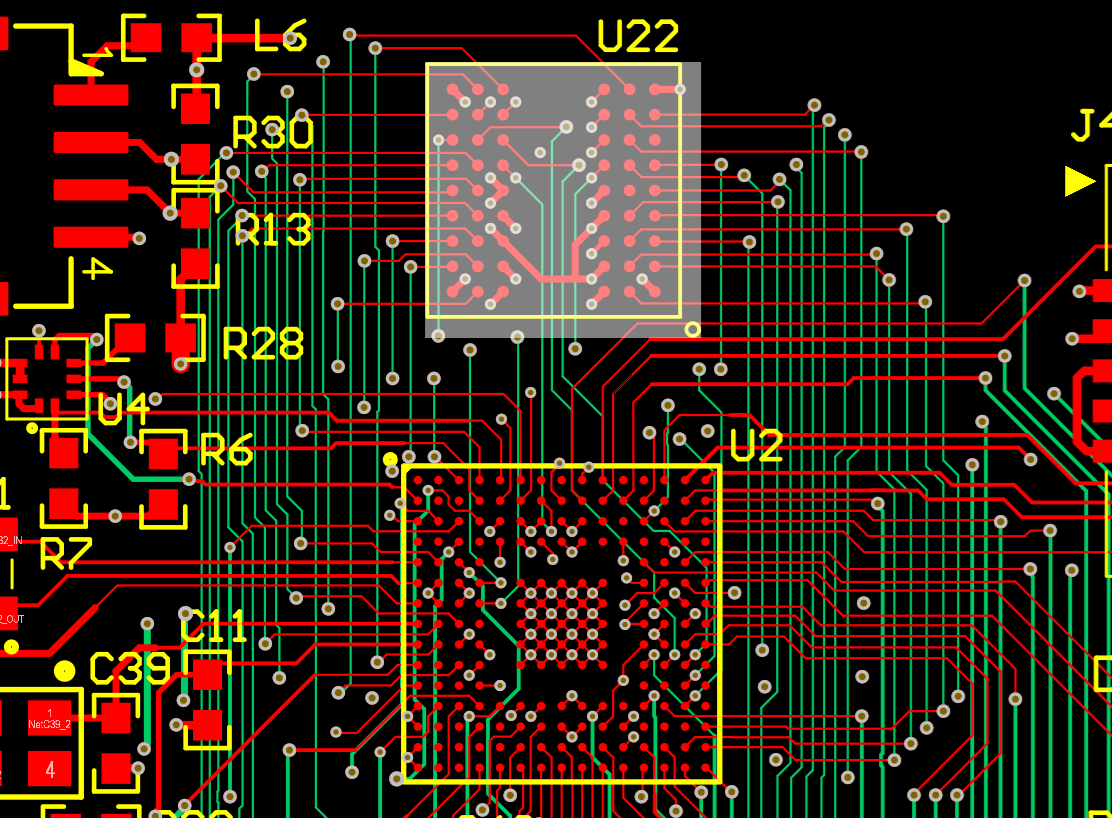
This parallel interface starts from a BGA (lower right corner) and routes into an add-in LCD module (upper left corner).
Strategy 2: Prioritizing Layers by Interface
In this strategy, specific impedance-controlled interfaces get their own layer assignments and are primarily routed in these layers. The manufacturer then takes a controlled impedance approach and determines the electrical properties that will be used when they build your stack-up. This type of strategy can be used when there are multiple high-speed interfaces requiring impedance control, and which may have different target impedance values. In some cases with differential interfaces, they have the same nominal impedance target but possibly a different bandwidth requirement, which will demand different line widths and spacing be used for the different interfaces.
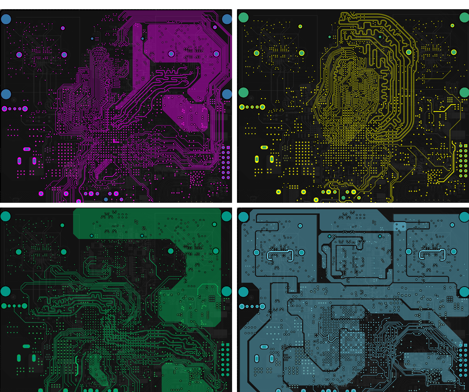
In the example images below, I show multiple digital interfaces assigned to different layers in a 16-layer stack-up. The interfaces involved are:
- DDR4
- CSI-2
- 1 Gbps LVDS
- 10 Gbps Ethernet
And see how these are separated into different layers in the plots below.
High-speed routing of multiple digital interfaces in a high layer count PCB.
You will notice that there is some empty space on these layers. It's important to remember that in this layer strategy, the primary goal is to make specifying impedance easier for the manufacturer. When there is only a single impedance specification per layer, it is much easier for the manufacturer to produce a stack-up that hits these targets for each interface.
The downside is that it tends to result in a higher layer count, as well as empty space on some layers. If needed, you can fill in some of the empty space with additional ground or copper for power rails. I prefer to use this space for power rails in some designs as it may allow me to completely eliminate a power layer. Also, you can still use these impedance-controlled layers for low-speed or configuration signals as long as they are not bunched up too close to your high-speed traces.
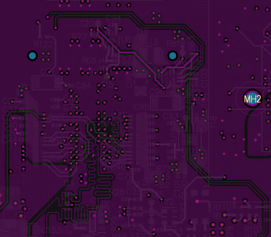
Strategy 3: High-Speed and Low-Speed Layers
In this strategy, the number of interfaces requiring controlled impedance is typically low, or all the impedance-controlled interfaces require the same impedance. This allows you to separate signals into dedicated high-speed and low-speed layers. This is similar to what you might do in a six-layer board with four signal layers, where your low-speed signal layers could be placed adjacent to each other.
This type of strategy is amenable to orthogonal routing, particularly if low-speed signals are present on adjacent layers. For example, see the routing shown below, which uses orthogonal routing directions between two components on two different layers.
These I/Os are part of an SDRAM interface and can be easily routed to the memory chip with an orthogonal routing approach.
The routing in this strategy will have fewer signal integrity challenges because many of the signals tend to be low-speed. Therefore, this approach helps maintain a reasonable layer count.
Strategy 4: Combine Power and Some Signals
Another routing strategy that I often implement in high-layer-count boards is to combine some signals and power rails into a single layer.
A common reason layer counts become high is not just due to a large number of signals or interfaces requiring routing. The layer count can also increase because of multiple power rails and power supplies. A novice designer might believe that a PCB requires a dedicated power plane for every power rail, but this would create a large number of layers with more copper than necessary. Instead, a better strategy is to use power rails drawn out as polygons.
In layers where power rails are drawn, it is acceptable to use those layers for routing signals. In particular, it makes sense to route lower-speed signals or configuration signals in these layers. I see many examples of this in the 1-Minute Design Review series, which looks something like the example routing shown below.
Routing in power layers is appropriate as long as large enough spacing is maintained.
This approach can be used within Strategy 2, as it allows you to utilize the remaining layers that are not assigned to ground for low-speed signals. High-speed signals can still get their own layers under Strategy 2 as needed. This helps keep the layer count from getting too high by eliminating the need for dedicated power planes and dedicated low-speed signal layers.
Additionally, it's still possible to route impedance-controlled traces in layers containing power rails. Typically, routing in a layer with coplanar ground requires enforcing a clearance rule to prevent excessive capacitance from affecting trace impedance. The same principle applies when routing near power rails. Instead of using a global electrical clearance rule, it's best to create a net-specific and layer-specific rule to enforce this clearance. In Altium Designer, you can set up this clearance rule using a custom query, utilizing the InNet (or InNetClass) and InLayer conditions.
Whether you need to build reliable power electronics or advanced digital systems, use the complete set of PCB design features and world-class CAD tools in Altium Designer®. To implement collaboration in today’s cross-disciplinary environment, innovative companies are using the Altium 365™ platform to easily share design data and put projects into manufacturing.
We have only scratched the surface of what’s possible with Altium Designer on Altium 365. Start your free trial of Altium Designer + Altium 365 today.

About Author
Related Resources
Related Technical Documentation
Table of Contents
Design to Release, Without the Friction
- Keep reviews tied to the right version
- Reduce handoff confusion and rework
- Spot sourcing and release risk earlier
- Work solo, share when needed
Get Started
Thank you, you are now subscribed to updates.

