Guide to Low-Dk PCB Materials


If you’ve taken time to learn about PCB material options and layer constructions, you have probably seen the wide range of materials that are available on the market. Materials companies produce laminates with varying Dk values, Tg values, weave styles, CTI values, and mechanical properties to target various applications in the electronics industry.
There is one set of materials that gets a lot of attention for its low-loss behavior: low-Dk PCB materials. These materials are often recommended for high-speed PCB design as a low-loss material option. However, not all systems need these materials, and there are other systems where the reliability of PTFE-based low-Dk materials may be much more desirable. Keep reading to learn more about the usage of these materials and how to make smarter material decisions for your board.
Standard Low-Dk PCB Material Options
In general, there are four broad classes of low-Dk materials that can be used in a PCB stackup:
|
|
|
|
|
|
|
|
|
|
|
|
|
|
|
|
|
|
|
|
|
|
|
|
These materials tend to have lower loss tangent than standard FR4-grade materials with higher Dk (ranging from ~4.2 to ~4.8). This is one reason why they are often recommended for use in high-speed PCBs, but this recommendation is often provided without the correct context. I’ll discuss some of the typical times to use low-Dk materials below. For now, let’s look at each of these material options:
Low-loss FR4
These materials are engineering epoxy-resin composite materials that are comparable in most ways to other FR4 laminates in terms of the primary material properties and constructions (glass weave/resin content, Tg value, mechanical properties). Two of the most popular vendors for these materials are Isola and ITEQ, although there are others that produce comparable laminates. These materials are used in a PCB stackup just like any other FR4-grade laminate would be used; the materials are available in prepreg and core options, and there are no major hybrid construction issues to consider.
- Dk value: ~3.7
- Loss tangent: 0.005-0.01
- Tg value: Low (~130 °C) and high (~180 °C) options available
- Thickness values: As low as 2 mil
- Copper options: Typically ED or RA copper
The glass weave styles in these laminates can vary greatly, from open (106) weaves to highly closed (2116) weaves and mechanical spread glass. For applications in high-speed, these laminates are desirable as they can be used with most high-speed protocols (DDR3+, PCIe, gigabit Ethernet, MIPI standards, etc.).
PTFE Laminates
The typical low-Dk laminate material that should be familiar to every designer is PTFE. These materials use PTFE and a curing agent mixed with ceramic fillers to engineer the dielectric constant, loss tangent, and Tg to certain values. These materials are also engineered to have very high Dk values for use in lower Dk applications (they still have lower total loss than FR4), as I’ve outlined in this article.
- Dk value: 3 to 10 with low dispersion
- Loss tangent: 0.0013-0.004 with low dispersion
- Tg value: Very high (~280 °C) but varies with material composition
- Thickness values: Some options below 5 mil
- Copper options: ED, RA, treated, or low-profile copper
The most-often cited applications for these materials are in RF systems operating well into the GHz range. Note that you don’t need to use Rogers for every RF board; below about 5 GHz (WiFi frequency range), the dielectric and copper losses in FR4 boards are just too small to be meaningful unless a board becomes very large.
This type of result can be clearly seen in Rogers dielectric loss data (I’ve cited multiple examples on this blog). You can also see this very clearly from simulation results, and from the analytical results I show in a blog on copper roughness.

Some PTFE-based PCB materials that offer low Dk may be available as unreinforced laminates, meaning they do not have a fiberglass weave reinforcement. For example, Rogers 3003 is one example of a very low loss tangent laminate with very smooth copper, and it is available without glass reinforcement. This eliminates the fiber weave effect, but it makes the material more difficult to work with when the laminate is thinner.
Liquid Crystal Polymer
This low-Dk, low-loss material is best-known for its use in advanced flex PCBs operating in the ultra-HDI linewidth/spacing range. These materials can be used with modified polyimides to form high layer count circuits, and they are often used in smartphones. Other application areas include high-reliability systems requiring elimination of a connector to prevent device failure, such as in aerospace systems.
- Dk value: ~3.1
- Loss tangent: ~0.002
- Tg value: High (~250 °C)
- Thickness values: Wide range
- Copper options: Low-profile/ED, typically low copper weight
To learn more about this class of materials, read this article by Happy Holden.
Polyimides and Bonding Films
These two sets of materials are used in flex or rigid-flex assemblies. Polyimides are the standard set of materials used in flex and rigid-flex layer stacks as board substrates. Some of the main material properties for these materials include:
- Dk value: 2.8 to 3.5
- Loss tangent: 0.003-0.01
- Tg value: Very high (>300 °C)
- Thickness values: Wide range
- Copper options: RA
Basic polyimide materials already offer slightly lower Dk values than most FR4 laminates, with the typical Dk value being approximately 3.4 for polyimides. Polyimides come in many varieties and product names, and their material properties vary by film composition. Note that there are some reports of low-Dk/low-loss polyimides operating in the GHz range. The paper below is one example of such a material.
Bonding films are one material that can be used in flex/rigid-flex PCB stackups to provide a low-Dk region above a copper signal layer. These films are very thin coverlay adhesive layers that are used to bond to the coverlay in a flex/rigid-flex PCB stackup. These films can have very low Dk value (less than 3) and very low loss tangent, but they are only useful in flex stackups as a low-loss coverlay adhesive. Other applications could make use of this material as long as it can be incorporated into a stackup. The typical material thickness is ~1 mil, so it only becomes useful in higher layer count boards.
- Dk value: ~2.5
- Loss tangent: ~0.002
- Tg value: Very high (~300 °C) but varies with material composition
- Thickness values: ~1 mil
- Copper options: N/A
To learn more about the reasons you should and should not use low-Dk PCB materials, watch the following video.
Ultra Low-Dk Materials (As Low As Dk = 2)
If you take a look around the RF world, you will find rigid circuit board materials that are very low, even less than Dk = 3. These materials are not often used in advanced HDI designs because they are not currently available in very thin layers (such as 2 mils or less). I alluded to these materials above in the section on polyimide, but polyimide is a thin flexible material being used as a buildup film in these applications, and does not get very far below Dk = 3.
Instead, we have to look to ceramic-reinforced PTFE to find materials that get as low as Dk = 2. Two solutions providers for these materials are AGC Multimaterial (inclusive of Nelco and Taconic), and Rogers Corporation.
As an example, take a look at the Rogers RT/Duroid 5880LZ data shown below. This laminate has very low Dk and Df values, which are very desirable in RF and digital systems operating at very high frequencies/bandwidths. Due to the available laminate thicknesses (as discussed below), the ideal applications for this material are still in the RF domain due to the required trace widths.
Unfortunately for digital systems designers, this Rogers material is not available in laminate thickensses below 10 mils. On a 10 mil laminate with Dk = 2, a 50 Ohm microstrip line would be 31 mils wide! A single-ended 50 Ohm coplanar microstrip with 10 mil trace-to-pour spacing would still be 27 mils wide. Obviously, this is a non-starter in advanced digital PCBs and substrates that demand lower Dk values as you would never be able to route into fine-pitch ballouts.
While digital systems designers using ultra-high speed interfaces (e.g., 224G PAM-4) would love to find rigid digital materials with Dk values as low as 2, the laminate world still has some catching up to do. Digital PCB and packaging designers would love to have a very thin rigid material with Dk as low as 2 as it greatly aids signal integrity in HDI systems. I know of one startup that is working towards this kind of material, and I expect the larger materials players to eventually follow suit.
Why the Focus on Low-Dk PCB Materials?
When many high-speed PCB design guidelines state to use a “low Dk laminate”, they will typically recommend a PTFE laminate. I have found two reasons for this recommendation, both of which are nonsensical:
- There is an incorrect assumption that low Dk equates to low loss
- The low-Dk equates to faster signal propagation, which is then used as an excuse to not match impedance or use a ground plane
The assumption in Point #1 is just plain wrong. Losses experienced by an electromagnetic wave are determined entirely by the imaginary part of the dielectric constant, not loss tangent. The loss tangent is just a summative metric that compares wave speed to wave loss, and it also simplifies some mathematical calculations involving distributed circuit element values for transmission lines. This all means that, for a given amount of dielectric loss, a lower Dk material would have a higher loss tangent than a higher Dk material.

This is something physicists learn on their first day in an optics class. For some reason, microwave engineers never got the memo.
The assumption in Point #2 is also a nonsensical guideline in high-speed PCB design. If you’re designing a high-speed PCB, you’ll spend a lot more time calculating trace lengths if you are trying to stay below the critical length for a transmission line. Also the “critical length” is not well-defined, as I’ve discussed many times. Therefore, you should just design to the required impedance for your interfaces, regardless of whether you are designing on a low-Dk or high-Dk material.
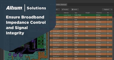
It’s also extremely easy to get an accurate estimate of the width that hits your target impedance. In addition to the Layer Stack Manager in Altium Designer, I’ve posted multiple calculator applications on this blog that can give highly accurate estimates near 50 Ohm target impedance.
Which Applications Need Low-Dk Materials?
Despite what I’ve written above about the guidelines about high-speed design, there are applications that do need lower Dk materials, including in high-speed PCB design. For example, the following applications commonly use a low-Dk material.
|
|
|
|
|
|
|
|
|
|
|
|
|
|
|
|
|
|
The low-Dk materials typically being used in these applications may be chosen because they happen to coincide with a lower loss tangent. Other boards, like high-reliability power electronics, might be built on PTFE or polyimide, but not because these materials have lower Dk value than standard FR4 laminates.
The last point in the above table is probably the most important for high-speed systems and in very high frequency systems. In both of these systems, small feature sizes will be required to hit target impedances and operate at the required wavelength (in RF systems). This means you can get to higher layer counts and operate at higher frequencies, but you will be able to use a less-precise fabrication process. This is arguably one of the greater advantages of these materials as more advanced products push further into the ultra-HDI range.
When you’re ready to select materials for your PCB stackup, including standard constructions with low Dk, use the complete set of product design tools in Altium Designer®. When you’ve finished your design, and you want to release files to your manufacturer, the Altium 365™ platform makes it easy to collaborate and share your projects. Come see the monthly feature updates in Altium Designer.
We have only scratched the surface of what’s possible with Altium Designer on Altium 365. Start your free trial of Altium Designer + Altium 365 today.


