


New Global Semiconductor Co-Investment Programs

At a Glance
The worldwide pursuit of semiconductor co-investment programs; a recap of the 2024 IEEE Electronic Components and Technology Conference (ECTC)


Applications that were once cutting edge, like artificial intelligence, quantum and high-performance computing, wireless and 5G communications and virtual and augmented reality, are quickly going mainstream, driving an increase in demand for the high-performance, low-power chips they require.
The need for new approaches to simultaneously achieve energy savings and performance gains to support these fast-growing, demanding applications has spurred increased interest and investment in advanced packaging around the world.
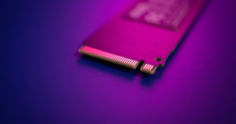
As BCG explains, advanced packaging essentially accommodates an ever-increasing number of transistors by decreasing the size of electrical contacts and is a crucial segment of the semiconductor industry. Advanced multichip packaging is one of the most significant new concepts in semiconductor design and manufacturing, integrating multiple components into a single package. This transformative approach departs from the traditional single chip per package model, directly addressing the most critical semiconductor technical and commercial constraints, enhancing performance and time to market while reducing manufacturing costs and power consumption.
Advanced packaging technologies, such as 2.5D and 3D packaging, provide greater flexibility in design and customization. This allows manufacturers to create specialized solutions tailored to specific applications and market needs. It also allows for the integration of different types of components, such as logic, memory, sensors, and RF modules, into a single package, enabling the creation of more complex and capable systems.
In short, advanced packaging plays a pivotal role in addressing the performance, size, power, cost, and integration challenges facing the semiconductor industry, enabling continued innovation and advancement in technology.

The Pursuit of Co-Investment Programs
The all-time high attendance figures for the 74th annual ECT, the world’s leading forum for advancements in microelectronics packaging and component science and technology, is a testament to the relevance of advanced packing in today’s market.
Worldwide, governments are increasingly pursuing co-investment programs with the microelectronics packaging and semiconductor industries to develop and expand infrastructure within their specific jurisdictions.
During the 2024 IEEE Electronic Components and Technology Conference (ECTC), representatives from Canada, the European Union, India, Korea, and the United States shared the diverse goals, frameworks, challenges, and achievements of their efforts to enhance advanced packaging technology and infrastructure.
While co-chairing the ECTC special session Exploring the Impact of Industry-Government Co-Investments for the Advanced Electronics Sector in North America, Asia and Europe along with co-Chair Erik Jung, Przemyslaw Gromala said, “Governments are striving to find ways to build their own semiconductor ecosystems in order to gain access to leading-edge technologies, to secure their supply chains, and to open up educational and employment opportunities for their populations.”
Przemyslaw also highlighted the influence of Biden’s CHIPS and Science Act of 2022, “The introduction of the CHIPS and Science Act in the United States has been inspiring similar programs elsewhere. The speakers in our lively special session detailed their programs and co-investments and also discussed the prospects of global collaborations and partnerships between national semiconductor and microelectronic packaging centers and industry leaders. They also outlined mechanisms for knowledge exchange, joint research initiatives, and mutually beneficial outcomes,” he said.

The Developing CHIP Ecosystem
The global semiconductor industry is complex and ever-changing. The ECTC offered an opportunity for engaged participants in the global advanced packaging industry to share their goals, varied strategies and implementation plans.
Here's what some of those participants had to say:
Canada
Established in 1984 as a non-profit organization through a collaborative effort involving 69 universities and colleges across Canada, CMC Microsystems facilitates connections between 10,000 academic participants and 1,200 companies who, together, collaborate on designing, constructing, and testing advanced prototypes.
During ECTC, David Lynch, CMC’s Vice President of Technology, presented FABrIC, an ambitious project exceeding $200 million over five years. This initiative, led by CMC and 14 other founding organizations, aims to accelerate the development of Canadian-made microchip manufacturing processes, Internet of Things (IoT)-based products and services, and quantum technologies.
FABrIC will leverage Canada’s existing advantages in compound semiconductors, micromechanical systems (MEMS), photonics, and superconductors as a starting point for growth, collaborating with experts in these fields to commercialize products and share Intellectual Property (IP) resources to foster a national semiconductor ecosystem, including relevant packaging strategies.
Europe
The European Chips Act, enacted in July 2023 and funded by the European Union, member states, and the private sector, has promoted substantial investments in cutting-edge fabs in Europe, although it has not specifically prioritized packaging.
At ECTC 2024, Elisabeth Steimetz, Office Director of the European Association on Smart Systems Integration (EPoSS), provided an overview of ongoing and potential initiatives in Europe. Among these is the progressing Pack4EU initiative, aimed at establishing a cross-European network for advanced packaging and creating a roadmap to enhance packaging capabilities across Europe.
EPoSS, an international non-profit governed by German law, spearheads the development and integration of intelligent and sustainable smart systems technologies and solutions for a sustainable society. It includes leading industrial firms and research institutions from over 20 European Member States, collaborating to formulate a vision and strategic research agenda to coordinate their efforts in these areas.
India
Rao Tummala, Advisor to the Government of India, highlighted the semiconductor industry landscape in India and its significant potential for development. He emphasized India's large and growing economy, numerous partnership opportunities among academia, industry, and government, a skilled and educated technical workforce, and the potential for global collaboration with academic experts from India and abroad.
Tummala also discussed the India Semiconductor Mission (ISM), a government-led initiative to strengthen India’s semiconductor ecosystem, stating that India's strategic R&D focus is on developing integrated semiconductors and systems packaging to serve large, rapidly growing markets.
Korea
Korea’s Chips Act, enacted in March 2023, offers substantial tax breaks and deductions for investments in the country's semiconductor industry. Kwang-Seong Choi from Korea’s Electronics and Telecommunications Research Institute outlined a packaging initiative focused on technology segments where South Korean companies excel, including 2.5D package-based high-bandwidth memory (HBM) optimization, 10-40 µm bonding, and hybrid bonding.
United States
In the U.S., the CHIPS for America Act passed in 2022 authorized $39 billion to attract significant investments in facilities, equipment, and manufacturing capacity for advanced technologies such as leading-edge logic and memory, as well as advanced packaging. It also allocated $11 billion for R&D programs aimed at enhancing semiconductor assembly, packaging, and testing capabilities.
One such program is the National Advanced Packaging Manufacturing Program, which aims to develop innovations to achieve U.S. technology leadership in advanced packaging for the semiconductor industry. At ECTC 2024, Eric Lin, R&D Director of the CHIPS for America Research and Development Program, discussed these programs within the context of the international landscape for advanced packaging. He outlined U.S. R&D goals and highlighted the extensive engagement with international partners in Asia, Europe, and the Americas to advance strategic objectives.
As a side note, the world’s leading high bandwidth memory (HBM) chip producer, SK Hynix, is set to build America’s first advanced packaging plant in Indiana for $3.9 bn.
“We are excited to become the first in the industry to build a state-of-the-art advanced packaging facility for AI products in the United States that will help strengthen supply-chain resilience and develop a local semiconductor ecosystem,” said SK Hynix Chief Executive Officer Kwak Noh-Jung.

About Author
Related Resources
Related Technical Documentation
Table of Contents
Design to Release, Without the Friction
- Keep reviews tied to the right version
- Reduce handoff confusion and rework
- Spot sourcing and release risk earlier
- Work solo, share when needed
Get Started
Thank you, you are now subscribed to updates.

