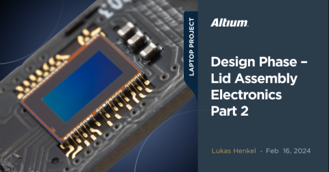


Design Phase – Lid Assembly Electronics Part 1


Milestone
1
2
3
4
5
6
7
8
9
Design Phase – Lid Assembly Electronics Part 1
| Created: December 20, 202310
11
More Milestones
| Coming soonWelcome back to the open-source laptop project series! In the previous update, we discussed how to integrate the various sensors and the electronics assembly itself into the bezel of the laptop display.
We’ve decided which PCB technology we would like to use, and what the mounting hardware for the webcam PCB looks like. In this update, we will focus our attention to the electronics and PCB design of the webcam module.

Fully assembled webcam/sensor PCB
Mainboard Interface
Let's start by figuring out how the webcam/sensor PCB should be interfaced with the mainboard of the system. We have four logical connections that have to be established with the motherboard:
1. Image sensor interface
The webcam, or image sensor interface, is first. The image sensor we will be using is an Omnivision OV2740. This sensor provides a high definition 1080p image at 60 frames per second. The image data stream is transmitted over a MIPI-CSI2 interface. A standard serial SCCB interface is used to control the sensor. A few global control lines are needed alongside this interface as well.
Usually, both internal and external webcams are connected via a USB interface that supports the UVC protocol. The UVC specification is short for USB Video Device Class and allows video streaming devices to be used without a hardware specific driver. This enables plug-and-play operation of external webcams. Another benefit of using the USB interface is that only one data pair as well as a power and ground connection is needed to interface with the device. This minimizes the amount of signals that have to be routed inside of the system which reduces connector complexity and increases reliability of the whole system. Another advantage of a USB UVC device or module is that it can be swapped with any other USB UVC compliant device which in the case of our laptop design would upgrade the webcam board to a newer version easily.
There is a problem associated with using a USB UVC compliant device in an open-source design, however: To convert the CSI output of the image sensor into an USB UVC compliant interface an ASIC with a custom firmware and ISP is needed. There are quite a few integrated solutions available from large IC vendors such as Realtek or SONIX Technology. The documentation for these ICs however is not freely available and therefore not the right choice for an open-source laptop.
One exception is the EZ-USB™ CX3 MIPI CSI2 to USB 5 Gbps Camera Controller from Infineon. This IC comes with accessible documentation as well as an SDK for designing a custom firmware for the image sensor. The EZ-USB™ CX3 however is catered towards USB3.0 applications for higher resolution or higher frame rate image sensors. With a price tag of greater than 10€ per IC in volume this component would be greatly over-specced for our application. Since this IC comes in a 10mm X 10mm 121 pin BGA, we wouldn't be able to fit it on the webcam board anyway.
So, for now, we will be routing the whole CSI2 interface provided by the image sensor directly to the motherboard. We have two options; either use the available space to implement our own USB UVC converter or interface the image sensor with the CPU/PCH directly and handle the image signal processing through firmware in the host CPU. At this time, the first option is more likely to be implemented. We will explore this more in-depth in a later update.
Other interfaces we need to route to the motherboard are as follows:
2. Microphone Interface
We are using two mems microphones in order to record stereo audio. These MEMS microphones provide a PWM (pulse density modulation) output that can be read by the PCH or embedded controller on the motherboard.
3. Ambient light sensor
The ambient light sensor provides an I2C interface that needs to be routed to the embedded controller on the motherboard as well.
4. Touch-Key Outputs
Last but not least, we have to route the output of the touch keys to the embedded controller. These outputs indicate to the embedded controller whether the WiFi or camera interface has been deactivated in hardware.
Board-to-board connector
Now that we know how many pins we need to allocate for the interface between the webcam PCB and the mainboard, we can choose a suitable board-to-board connector. In order to keep the space needed for the connector as small as possible we will use a fine pitch connector.
For this version of the webcam board, we’ll use a Molex SlimStack 505550 connector with 40 pins at 0.4mm pitch.

Molex SlimStack connector
We will be using a double-layer FPC to route the signal from the webcam PCB to the mainboard. While the SlimStack connector is a space-saving solution, the testing has shown that unplugging this connector is very difficult while the display panel is sitting on top of the FPC.

FPC connected with display panel installed on top
To make it easier to swap the webcam PCB with the display panel installed, we will swap out this board-to-board connector with a direct FPC connector. An interesting candidate for such a connector might be the Hirose FH35C series which features a very high pin density as well as good retention force.
Capacitive Touch Sensors
The capacitive touch sensors TTP232-CA6 used on the webcam board are dual channel sensing ICs from Tontek. Since one chip provides two channels each IC handles sensing both the activate and deactivate button for the Webcam, WiFi and Microphone functionality.
On each input of the sensing ICs an optional capacitor in an 0201 footprint is placed. The sensitivity of the touch IC can be tuned with these optional capacitors.
Following the sensing ICs a latch is used to store the last button press. In the current implementation of the latch the device starts up with the camera, WiFi and microphone functionality deactivated upon power-cycle. Especially for the WiFi functionality this behavior might be undesirable which is why the default state for this channel might be inverted later on.

Touch sensing channel for the WiFi functionality
Microphone and ambient light sensor
The microphones and ambient light sensors that we´ve selected in a previous project update were implemented according to the datasheet. Both sensors are supplied from a separate 3.3V LDO that provides a supply voltage generated from the 5V input power that is routed to the webcam board.
The ambient light sensor is located on a small add-on board that contains a decoupling capacitor and the I2C bus pull-up resistors.

Microphone and ambient light sensor
Webcam image sensor
The webcam image sensor is implemented as follows. The power rails for the sensor are all generated locally by three small LDOs. The TLV740P LDO series is a very space-saving and cost-effective solution. The package used is the 1mm X 1mm X2SON which results in an overall very small solution size.
The power draw of the image sensor is low enough that every power-rail can be generated by dropping the global 5V rail down using linear regulators.

Webcam image sensor schematic
Webcam board schematic
The finished draft of the webcam PCB schematic can be seen in the Altium 365 viewer:

Besides touch-keys and sensors, the webcam PCB also contains a RGB LED for each sensing channel output. RGB LEDs were chosen in order to be able to fine-tune the color of the backlit icons by altering the resistor value used for each single color.
A small logic level N-Channel MOSFET in a SOT-883 package is used to apply a global PWM dimming to all LEDs on the webcam board. The same PWM signal that will be used to change the brightness of the screen can be used to also control the LEDs for the backlit icons in the screen bezel. This way the icons won't be distracting in case a low screen brightness was chosen.
With the schematic finished, we can now pass all the information into the PCB editor and start routing the board.
Stay tuned for the next update, where we'll provide valuable insights into the PCB layout of the webcam board—don't miss out on the latest details that will enhance your understanding of the design and functionality!

About Author
Related Resources
Related Technical Documentation
Design to Release, Without the Friction
- Keep reviews tied to the right version
- Reduce handoff confusion and rework
- Spot sourcing and release risk earlier
- Work solo, share when needed
Get Started
Thank you, you are now subscribed to updates.

