The PCB Design Process Methodology and Application

Your next great idea probably started on a piece of notebook paper. How do you go about taking your great idea and turning it into a real design, and eventually into a finished product? There are a number of ways to approach your new design. Any new circuit board can be very complicated, but the right PCB design process methodology helps you get through the design process quickly.
PCB designers follow a general PCB design process methodology, and there are some important things to consider in your schematic and layout before you get started. Who will be using your circuit board? Where will it be used? Which aspects of its environment will affect its functionality? Thinking about the answers to these questions can help you avoid common problems in PCB design process methodology and determine the right PCB design process methodology for your next idea.
PCB designers used to be forced into using multiple programs with a rigid workflow to create a schematic and PCB layout. Now, innovations in PCB design software allow PCB designers to create a PCB design process methodology around complex key features in their circuit board layout. Powerful routing tools, schematic simulation features, and ECAD/MCAD collaboration features help keep PCB designers productive and building advanced printed circuit designs.
Once it comes time to lay out your circuit board, you’ll need to adopt a methodology that ensures your signals remain free of common problems, your board is manufacturable, and that you have followed important design rules. The right PCB design software with design rule checking features throughout the schematic and layout phases will help ensure your printed circuit boards can be manufactured properly and will function as designed. You can take advantage of the functionality and power of PCB design software applications such as Altium Designer available within Altium Develop to create advanced printed circuit designs with ease.
Key Takeaways
- A strong PCB design process starts with understanding the end use and environment, then selecting and sourcing components and building a clear, well-organized schematic.
- Simulation-driven design at the schematic stage helps validate circuit behavior, improve signal/power integrity, and reduce redesigns before layout.
- During layout, defining stackup, routing rules, and design constraints (plus running post-layout simulations and DRC) ensures manufacturability, signal integrity, and fewer errors.
- A unified, rules-driven platform like Altium Designer within Altium Develop streamlines schematics, layout, simulation, and manufacturing documentation in a single environment, boosting productivity and reliability.
Schematic Design: The First Step in the PCB Design Process
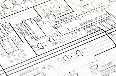
Once you’ve got a basic idea for your board, it’s time to start creating schematics that show how components are connected throughout your printed circuit board. Your schematic is the first document you will create when you want to create a real model for your entire product. Your schematic will show all connections between components (both single-ended and differential) that will appear in your circuit board.
Having access to components sets the stage for placing the components on the schematic and for wiring the circuit. Well-structured and detailed design notes also assist with determining signal integrity and power integrity faults with the design. Your PCB design process methodology begins with selecting and sourcing components, followed by creating schematics that show electrical behavior.
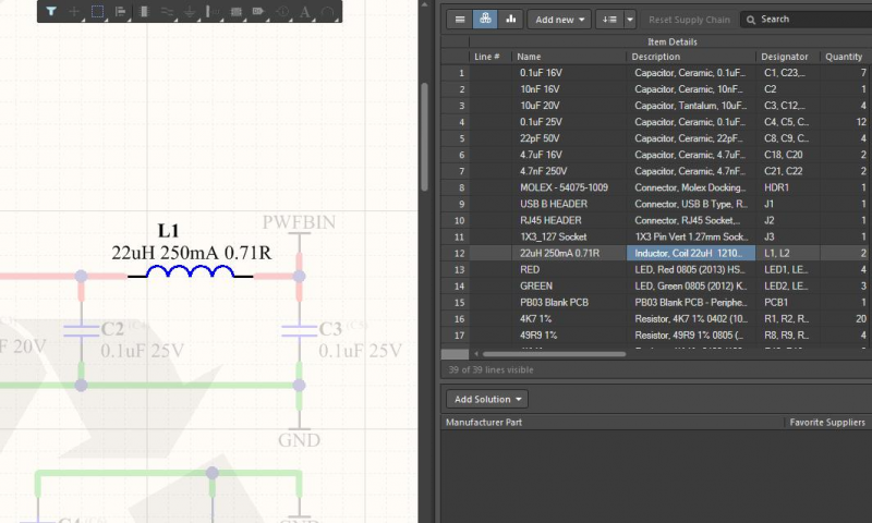
Selecting components for your schematic in your PCB design software
Simulation-Driven Design in Your Schematic
Some designs will require simulations as an application of the PCB design process methodology, especially if you are not using well-known circuits, making creative use of active components, or working with proprietary components. With the right simulation package, you can evaluate circuit functions before you create your PCB layout. This can help you explore the effects of transients in your interconnects and components, address undershoot/overshoot, and plenty of other performance aspects of your circuit board design.
Some components, like printed circuit antennas or external antennas without impedance matching or filtration, will require simulations to design an appropriate impedance matching network to support circuit board signal integrity. You can take a simulation-driven approach to help you design supporting components to ensure signal integrity before you finalize your schematic. This PCB design technology will help prevent some unnecessary redesigns after you start laying out your PCB layout.
- Your schematic will be the first design document you need to create before you start building your printed circuit board.
Learn some design strategies for getting started with schematic design.
- Working with hierarchical schematics is a great way to stay organized when designing your schematics. This design methodology allows you to define parent-child relationships between different functional blocks in your schematic and PCB layout.
Learn more about enforcing organization with hierarchical schematics.
- Integrated PCB design software will allow you to create circuit models from your schematic for mixed simulations during the design process.
Learn more about creating simulations from your schematics in your PCB design software.
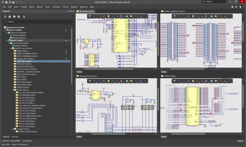
Schematic organization helps you create the right PCB design process methodology.
Your Printed Circuit Board Layout Process
After you create schematics and verify electrical functionality with simulation tools, you need to define your layer stack, which will show the arrangement of signal layers, each power plane, and each ground plane. When you’re ready to start arranging components and route traces throughout your PCB layout, you can define routing rules and constraints within your PCB design software on any of the key features in your printed circuit design. These design rules and constraints can be defined around specific industry standards that govern manufacturability and functionality. This helps ensure that you do not make any errors while creating your PCB layout.
Get to Fabrication with Post-Layout Simulations and Documentation
As you create your PCB layout, your PCB design software should check your routing and layout against the design rules and constraints you define. This helps you catch errors early and prevent them altogether. When you’ve completed your layout, you can use post-layout simulations to verify signal integrity before you create manufacturer deliverables for your fabricator.
- The best PCB design software programs include PCB layout and routing features that can be accessed alongside your schematic drawings. Working in a single PCB design program helps you stay organized and productive.
- Design rules are also intended to help ensure signal integrity throughout your board. You’ll need to place verifiable test points on your board during the design phase.
Learn more about signal integrity in your PCB with Eric Bogatin.
- Once you’re ready to manufacture your circuit board, it helps to have an understanding of the manufacturing process and how manufacturers will use your design data.
Learn more about the manufacturing process and how manufacturers use design data.
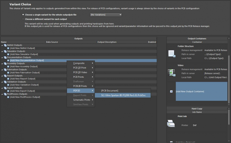
Create your manufacturing deliverables within your PCB design process methodology.
Create Your PCB Design Process Methodology in Altium Designer
The unified design rules-driven environment in Altium Designer lets PCB designers easily create schematic drawings, a PCB layout, and manufacturing documentation in a single environment. After configuring your printed circuit board workspace, layers, grids, and design rules, your design team can arrange components and route traces throughout a circuit board layout. The PCB Editor supports the 32 signal layers, 16 internal power plane and ground plane layers, and 32 general purpose mechanical, special, and non-electrical layers. Altium Designer displays attributes for all layers in a color-coded workspace. You’ll have the best PCB design technology on the market when you use Altium Designer available with Altium Develop.
Stay Productive with Unified PCB Design Software
Because your PCB design process occurs within a seamless, unified environment, your team can easily move from creating a project to full-scale production. Every function in Altium Designer is built on a rules-driven engine, allowing PCB designers to apply design rules to a project and ensure electrical functionality. Moreover, Altium Designer provides tools for automatically compiling extensive manufacturing documentation, including Gerber files, design notes, and bills of materials. The key features in Altium Designer can be viewed in extensive tutorials, and you'll have access to plenty of schematic design and PCB layout resources to create your board.
- The design rules-driven engine in Altium Designer helps you automatically spot errors in your schematic drawings and PCB layout. You can stay productive and design powerful electronics in this unique design environment.
Learn more about the unified design rules-driven environment in Altium Designer.
- When you’re ready to manufacture your PCB, you’ll have the tools you need to produce manufacturing and assembly documents. This includes everything from solder mask definitions, to power and ground plane arrangement, to instructions for pick-and-place machines.
Learn more about producing manufacturing documentation in Altium Develop.
- Altium offers many PCB designing tutorial resources for new designers through the Altium Academy.
Learn more about using Altium Designer through Altium Academy.
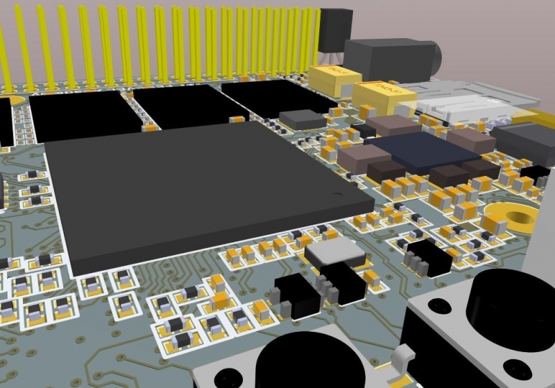
Integrated 3D modeling for printed circuit board design makes Altium Designer stand out from the rest.
No other PCB design software platform gives you this many tools in an easy-to-use interface. For your PCB designing tutorial, Altium gives you access to on-demand webinars, design tutorials, and the AltiumLive forum. You’ll have the tools and resources you need for successful printed circuit board design in Altium Designer.
Whether you need to build reliable power electronics or advanced digital systems, Altium Develop unites every discipline into one collaborative force. Free from silos. Free from limits. It’s where engineers, designers, and innovators work as one to create without constraints. Experience Altium Develop today!

