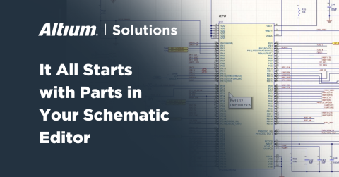


Easy Schematics Creation for Elegance and Readability

At a Glance
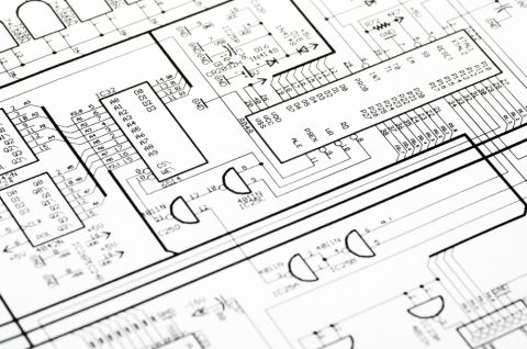
Exemplary schematics will show you the circuits plus everything you need to know about them at a glance. Poor schematics will force you to decipher them to glean a sufficient understanding of what the circuits do.


A schematic drawing will not only tell your PCB design software what needs to connect where, but it also communicates the purpose of a circuit to other people. It’s easy how to make schematics, but it can be harder to make helpful schematics that can be quickly and easily read and comprehended by the reader. Anyone reading your schematic diagram should not have to try and trace wires around to figure out what they do or need to unscramble a tangled mess of interconnections in their heads.
In this guide, based on years of industry experience, we will show you how to improve your schematic layout so that your designs are elegant and readable. The Oxford English dictionary defines elegant as:
- Graceful and stylish in appearance or manner,
- Pleasingly ingenious and simple.
In our view, schematics should meet both of these definitions, and by creating schematics that are simple, graceful, and stylish, you should automatically make something readable. We’re not talking about adding flourishes or artwork to your schematic, just about how symbols and components are simply connected, labeled, and laid out on the schematic sheet.
Easy Schematics Flow
So, how to read a schematic? At a very high level, schematics across most of the “western world” are read from left to right, the same as we read the text in our languages. We don’t have any experience with reading words from right to left as used in some languages, so we can’t speak for how a schematic should be best laid out for people working in these regions. Signals flow from left to right, and voltage potentials generally (for voltage regulation) decrease from left to right. Currents usually flow from top to bottom.
At a very high level, this is often captured in a block diagram, and the signal flow rule applies at the block diagram level. Within each block, the signal flow rule also applies so that the path of signals and power is very easy to trace throughout the system. For example, this block diagram showns all of the important parts of a system, as well as signal flow to some of the main components in the design. The use of hierarchical schematics allows a similar block diagram structure to be created.

There are, of course, exceptions to this convention. For example, a boost regulator will provide a higher output voltage potential than its input voltage potential, but we still expect the output to be on the right-hand side and the left-hand side’s input. Following this left-to-right logical flow will be consistent with the reader’s expectations.
Readers should find objects where they expect them to be if to create schematics to meet the readability criteria. Connections for inputs should be on the left, flow through your schematics symbols, and then appear as output connectors on the right side of the sheet.
Nets and Ports
One of the things often seen in the “Typical Application” schematics in a data-sheet is a complete lack of power ports. Everything is connected with net lines, and having your ground and power nets snaking around your schematics to connect to every pin that connects to the power ports makes them very hard to follow. Instead, we recommend you use local power ports to show the connection. Nets wires should contain signals, and power nets have no signals carried on them. By removing power nets to prevent them from appearing all over your schematics, you instantly declutter them only to show the relevant connections needed to understand the schematics.
Nets should always have names. This is required for the schematics and the PCB design - in Altium, the netlabels show up on the pads and tracks. A PCB track labeled NetIC2_14 doesn’t help us understand what that track is going to do or what signal it might carry - therefore, it’s not immediately apparent what the current might be or what speed the signal might be. In the schematic, name all your nets; it will make life much easier for the PCB layout and enhance your schematic’s readability. When it comes to devices such as microcontrollers and other logic devices where pins have multiple functions, the net names immediately make a schematic diagram simpler to read. Rather than following a net wire from the microcontroller port PB4, off to where it connects, we can read right next to the microcontroller’s schematics symbol that this is “BTN1,” indicating that it is for button 1.

Remember to keep the net names short. Not only does it save you a lot of typing, but it also makes the names easier to remember and much easier to read on a PCB pad or track. A net labeled USER_INPUT_BUTTON_1 is less helpful than BTN1, as, on the PCB, you might only see USER_IN… or perhaps not even that much of the name. Long names also unnecessarily clutter up what should be a clean and easy schematic sheet. It is also recommended that you use uppercase for net names. It removes ambiguity, for example, over whether a character is an ‘I’ (upper case i) or an ‘l’ (lower case L), or a ‘1’. Uppercase letters also tend to have more consistent widths in non-fixed-width fonts, which means as you read down a list of net names, they appear aligned and a little more readable. The final case for using uppercase is that it makes the net/pin/component designators stand out in the documentation or any written discussions about schematics. See the Altium Library Standard Pin Name Abbreviations document for a terrific list of abbreviations for common names.
Power port names should also be kept as short as possible; try not to let them get much more comprehensive than the port symbol itself. This makes PWR_IN better than INPUT_POWER. Try to describe the electrical function first for power ports, followed by its use case. This means if you are looking at a small pad on a capacitor, for example, you can still see that one pin is PWR and the other is GND. If we had our input ports labeled INPUT_GND and INPUT_PWR, we might only see “INP...” on the pad or track, which creates ambiguity. You should always avoid any ambiguity which could lead to layout, routing, or connection mistakes that would need to be fixed later - hopefully before ordering your boards! If you need to have decimal places in your power port name, such as ‘3.3V’, keep it consistent. We recommend replacing the decimal with the units, so in this case, ‘3.3V’ becomes ‘3V3’. The reasoning is that it is much easier to misinterpret ‘3.3V’ as ‘33V’ than it would be with ‘3V3’, especially if you have your schematics printed or displayed on a small screen. It’s crucial to pick a standard way to represent your voltage rails and stick with this throughout the design.

When placing power ports, keep their orientation consistent. Try to keep higher potential symbols with the net connection coming out the bottom and lower potential symbols with the net connection coming out the top. Labels such as VCC, 5V, and 3V3 should all be positioned above the symbol and oriented to look like a T-shape. Conversely, VEE/VSS/GND labels should always be set below the symbol, and negative voltages should be oriented the same as your GND. Never have your power ports orientated sideways or upside down - you should be able to tell the polarity of a power port’s connections just by looking at it.
Harnesses
In Altium, harnesses are a powerful tool for taking a group of connections from one sheet to another in a hierarchical design. Rather than creating ten separate ports for a set of connections that go over to another sheet, we can use a single port symbol with a single net connection between the two symbols in our higher-level schematics.

Easy Schematics Layout
If your schematics have more than one logical group of components, you’ll need to split the schematics into multiple sheets - we’ll get into that in more detail later. Using the hierarchical design features of your EDA package will allow you to build a block diagram on your higher-level sheets using the sheet component blocks. If it’s a particularly complex device, you may need to have many layers for the design, with each top-level sheet for that layer/level getting more specific and detailed. This may initially take a little more effort than having a project full of random schematic sheets. Still, it documents your product at a block level very clearly, showing how the logical groups of components interact with each other.

This can save time determining how a single schematic sheet interacts with the rest of the product by allowing you to simply look at the block diagram to see where the off-sheet connections/ports go, without necessarily needing to view the destination/source sheet in detail.
Logical Separation
Altium has fantastic support for multi-sheet schematics and hierarchical schematics – we recommend taking full advantage of these features. We like to use one easy schematic sheet for each design’s logical function, so every isolated block in the design will be standalone. We see many open-source designs drawn using Altium or other EDA software that comprise one giant sheet with lines drawn between each block to separate each section logically. In Altium, we can do this much better. If we need to export these schematics to someone else or print them out, all the relevant components for each logical block can be on a single page. The page does not need to be scaled down to fit everything on our printed schematic, making the drawings easily readable. When viewing schematics on screen, we can take everything relevant in with a single view; we don’t need to scroll around the sheet trying to find where something connects. We can simply switch to the sheet that contains just those components of interest.

Try and stick to using regular paper sizes that are readily available in your country. If you’re in North America, use Letter/Tabloid schematic symbol templates. If you’re in most of the rest of the world, stick to A4 and A3 sizes. You could use a paper size that needs a plotter to print, which means you could fit everything on one sheet, but as just discussed, that’s not very practical. It also does not make your design very portable.
Spacing
When thinking about how to make reading your schematics easier, it’s essential to give your symbols room to breathe, at least wherever possible. I like to provide at least 1 grid square of space, but preferably two, between all pins, symbols, and labels. If everything is jammed too close together, it’s much harder to follow. This goes for designators and values text as well; you should leave plenty of room between all the graphical elements of your design. As a reader, you will want to evaluate each entity on your schematic by itself, without having other components crowding in and making it harder to read.
Conversely, you should not have your components too far away from each other. If you have components too far apart with long net lines spanning between everything, not only will you clutter your schematics, but you will logically separate these components from each other. Components working together for a single purpose, such as decoupling capacitors for an integrated circuit or feedback resistors for a voltage regulator, should be kept together. This is so that the main component and its supporting components can be viewed and evaluated as a single unit.

Keep groups of components together that belong together, so you only have wires leaving that group, which connects to a separate group of components. Each group of components should have everything they need to operate and affect the signals that leave the group. Any signals leaving the group should go to another group with a separate and distinct function of its own.
Symbol Orientation
We’ve already talked about the orientation of power ports, but the same rules apply to the other standard schematic symbols as well. If you’re using a device with an industry-standard schematic symbol such as a transistor or MOSFET, keep it oriented the way everyone expects to see it. If you flip your P-Channel MOSFET upside down, it could easily be confused for an N-Channel MOSFET at first glance, which obscures your design’s original intent.
This rule’s key exception is two passive pin components: resistors, capacitors, inductors, or even LEDs. These are all easily recognizable in any orientation and should be positioned so that they make your circuit as easy to read as possible.
Schematics Symbols
We have produced another article specifically about the creation of usable schematic symbols. However, for this article’s purpose, I’ll condense it down to one fundamental rule: Schematic symbols for integrated circuits should rarely if ever, match the physical pinout of the device. Easy schematics are about the signals and should be readable; how the pins of a device happen to be set out on the package/die will have no relation to how readable a schematic symbol is. Unless you’re fortunate, trying to use the pin layout that the physical package uses is likely to leave you with a messy schematic with wires crossing all over each other. Make sure you arrange the pins to make your schematic as straightforward as possible.
Easy Schematics Documentation
When it comes to things like simple calculations, prior revisions, and the sum of all data in your schematics, it can be a great addition to include these as explanatory texts.
Release notes, revision histories, and tables of contents are very useful for navigating schematics. This is especially true when collaborating with non-ECAD engineers as they will not be working in the schematics in your design tool. Most often, they will be looking at a PDF of your schematics, so any documentation that can be included will be helpful for navigating the schematics and understanding the design intent.

Another example that is very useful in power electronics, embedded systems, and some RF systems is to include a power sequencing diagram. Power sequencers provide a passive method for managing the power-up stage of a system, with specific timing schemes being implemented in with a set of discrete components or a sequencer IC. If this is present in the design, a simple diagram like the one shown below will give a test engineer an idea of what to expect when the system is powered on.

Some other examples of simple documentation in schematics include:
- If you have a voltage divider in your schematics, add using your documentation color (I typically use purple) descriptive text like “5V = (1 + (R2/R1))1.25V” next to the resistors. This will let anyone reading the schematic know that when there is 5V on the top resistor, they can use the values of designators R1 and R2 to calculate the 1.25V value at the center point of the divider.
- If you have LEDs in your schematics, add a note near the current limiting resistor or LED (since they should be right next to each other) that notes the expected current. A description along the lines of “2.1Vf, 20mA” is sufficient for someone checking your schematic or looking at the expected current draw for the device.
- If you have an operational amplifier or instrumentation amplifier in your design, add a note to show what the gain is to save someone (perhaps you in the future) having to calculate the gain value, making debugging easier.
If you’re using a quality component library to create your schematics, you should use the parametric data available for each added component rather than generic symbols. Place the actual part into your schematics rather than a generic resistor or capacitor symbol and then assign it with the appropriate resistance or capacitance. Generally, you should only have the component designator and value displayed. However, if you have a particular case where you need to use a specific tolerance, dielectric type, or other critical information, then enable the display of the relevant parameter. This component has a particular parameter displayed when the others do not call the reader’s attention to the specification when purchasing, testing, or debugging the hardware.
Do Your Best
The best advice we can give is to try your hardest to make the schematic understandable to others or yourself if you return to it in the future. Exemplary schematics will show you the circuit plus everything you need to know about the circuit at a glance. Poor schematics will make you need to decipher it to understand what the circuit does.
You should aim to create, at the very least, something that looks neat and tidy. The layout should not obfuscate the details in a jumble of wires or a crowd of components and text. Like how good circuit routing is aesthetically pleasing and looks like a work of art to us engineers, the same should also be said about your easy schematic designs. Well-drafted schematics will look elegant and beautiful, and by achieving this, they will be easily readable and straightforward to understand.
Have more questions about how to read schematics? Or making an easy schematic to read? Call an expert at Altium and discover how we can help you with your next PCB design.
About Author
Related Resources
Related Technical Documentation
Table of Contents
Design to Release, Without the Friction
- Keep reviews tied to the right version
- Reduce handoff confusion and rework
- Spot sourcing and release risk earlier
- Work solo, share when needed
Get Started
Thank you, you are now subscribed to updates.

