


What Is Schematic Capture?

At a Glance
All designs start with creating schematic sheets for your circuits. Learn more about what is schematic capture in our guide for new engineers.


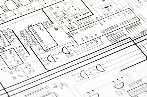
In simple terms, schematic capture is the process of converting a paper design into an electronic representation that software tools, such as circuit simulation or PCB design packages, can process. Graphically, schematic capture (also known as schematic entry) is the process of arranging components in schematic sheets and defining links between them. In this way, you produce a logical/electrical design that can be used in your other design tools when you're ready to run simulations or create a physical layout.
Behind the scenes, your design software doesn't really care about how you arrange components into schematics. Circuit simulation packages like SPICE and your PCB layout tools only care about the connections you define between pins on different components. These connections are called "nets," and schematic capture is really the task of creating a list of nets that will be reflected in the make up everything in your physical PCB layout. The graphical interface you see in your schematic editor software helps you stay organized as you create your design and eventually transition your designs into a PCB layout.
Schematic Capture: Basic Principles
A circuit diagram is fundamentally a list of parts and the links between the connections of those parts. These can be electronic components from a simple resistor to a complex integrated circuit chip or FPGA—alternatively, mechanical components such as connectors, dials, or switches.
The schematic capture process needs to include everything within the circuit design necessary to work, including the electrical connections with its environment. Thus, attention to detail is vital; any omissions in the circuit design captured schematically can cause headaches down the line when things don't work as expected and potentially costly diagnosis and corrective actions.
The output of the schematic capture process is generally in the form of a netlist that can be imported into other software tools, such as a simulation program or PCB design package. Some design programs force you to manually export and re-import netlists each time you modify something in the design, which will re-synchronize your project to ensure your schematics and PCB layout show the same set of connections. With other design software, you never see a netlist file: the design software handles this synchronization automatically so that you can quickly move into your PCB layout.
Rules of Thumb
During schematic capture, you'll be working in a graphical interface, where component models are placed in drawings and connected with wires. There are a few basic practices that can help you save time and ensure your schematic sheets are easy to read:
- Components should be placed so that signal flow spans from left (input) to right (output). Likewise, power supplies should feed from top to bottom, meaning power ports should be placed at the top and ground should be placed at the bottom. This convention ensures that anyone looking at the schematic will immediately understand where signals pass to and from, and which lines carry signals and which carry power.
- All labels should follow a consistent naming convention to help the reader understand and highlight potential problems. For example, a connection labeled as a power supply line but positioned as a signal line will stand out immediately, making it easier to debug a circuit design before layout and manufacturing.
- Lines should not cross or converge where possible to avoid confusion. Crossing wires creates the appearance of a connection between lines, although this may not be the intent. Using universal symbols for power supply connections can reduce the number of lines and make the schematic clearer. If lines do need to cross, make it evident to the reader that this is the case. If lines join, limit this to a maximum of three lines. More than three lines meeting at one point could be mistaken for unintentionally crossed lines.
- If the schematic is so large that it covers multiple pages, separate components so that each page has complete functional blocks rather than randomly placing these blocks across pages. Connections, where lines flow between pages, should be identifiable. Some design software will use an object called a "port" to denote a connection between two different sheets; this is a best practice that makes clear a connection is being made to a different schematic sheet.
- Don't forget that some components need additional parts that aren't part of the functional design: decoupling capacitors, line filters, and lightning (ESD) protection. A host of components that a device requires to operate in the real world are not built-in, and they need to be added as external parts. However, forgetting to include these in the schematic capture will invalidate circuit simulation results and may cause the finished product to be non-functional.
- Finally, if any aspect of the schematic is unclear, add an explanatory note. You'll thank yourself later when you look back at the schematic and can't remember some of the design decisions you made at the time. If you're working on a team, your team members will also thank you as the intent of the design will be clear.

What's Needed in Schematic Symbols?
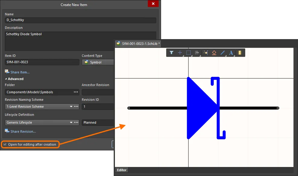
Each of the schematic symbol elements above needs to include specific information relating to the system design and creation of the PCB layout. Schematic symbols are first created in libraries, and this is where the important information needed to create a PCB is located.
The important information that a designer should place in a schematic symbol includes:
- Manufacturer and manufacturer part number
- Preferred distributor and distributor's part number
- Footprint found in one of your footprint libraries
- Component type (standard, net tie, no-BPOM, etc.)
- Component value or type of component
- Basic operational ratings (temperature range, current limit, etc.)
- Simulation model, if available
The first four points are mandatory for every component that you will use in a PCB. This data is bare minimum information required to order the component and place the component in the PCB layout. While there are many other pieces of information that could be included, it is not required for the component to simply be placed in a PCB layout and then exported into a BOM.
Component information set in the Properties panel in Altium.
The last point above relating to circuit simulation is not mandatory, and it is only important if you plan to perform circuit simulations in your schematic capture tool. For example, many schematic capture tools include an embedded SPICE simulator, but the SPICE simulator only works if the components being simulated have SPICE models attached to them. While SPICE models are also not required, SPICE simulations are often an important part of engineering and schematic capture as they give you the chance to qualify design performance before a design is finalized.
Circuit Simulation
Simulation tools are used to take a schematic design, stimulate the inputs, and monitor the theoretical outputs. These tools allow the designer to test a circuit diagram or groups of circuit designs under all possible input conditions, verify the circuit operates as expected, and validate the circuit against the overall requirements for the device it implements. The standard simulation tool is SPICE, which is built into most schematic editor applications.
Each component and input signal included in the schematic needs its operating parameters and performance characteristics defined. Although details for standard components are often available in libraries of data, bespoke or unusual components may need this information defined and entered manually. Remember, a simulation will only be as good as the data it uses. Any errors, however small, can lead to misleading or unrepresentative results that may only become apparent when the assembled device is operating.

An important point to remember is that simulation tools tell you what the circuit will do under perfect conditions. Therefore, unless added to the model, they won't consider real-world effects such as trace losses due to impedance or generation of radiated noise. In addition, it won't take into account interference from received radiated or conducted noise emissions, cross-talk between signal lines, and other indirect effects. A good designer will investigate the susceptibility of their circuit design to such factors and feed these into the PCB design as constraints that translate to trace minimum width and maximum length parameters, trace separation constraints, and shielding/screening requirements.
Transition to PCB Layout
Once your schematics are finished and you're ready to start the PCB layout process, your design tools can help automate the transition into a physical design. Rather than exporting a netlist from the schematic editor and re-importing it into a PCB editor, the best tools can bypass this process and can directly import your component data into a new PCB layout. However, always double-check each circuit diagram in your schematic sheets before committing to manufacturing the board. Most packages include rule check features that can uncover easy-to-miss errors like opens and shorts. These aren't a substitute for a manual schematic design review.
To answer the question of "What is schematic capture?" – it's a process that allows the designer to simulate their circuit to validate their design and then create an optimum PCB layout with minimum effort. However, at each step of the process, the designer needs to perform careful checks to prevent errors affecting the following steps. Simulation tools and PCB design packages can make the designer's life easier by automating the transition from schematic sheets into a PCB layout. Still, they are never perfect, and the designer should never rely on the outputs of a tool without thoroughly reviewing them.
Whether you need to build reliable power electronics or advanced digital systems, use Altium’s complete set of PCB design features and world-class CAD tools. Altium Develop provides the world’s premier electronic product development platform, complete with the industry’s best PCB design tools and cross-disciplinary collaboration features for advanced design teams. Experience Altium Develop today!
About Author
Related Resources
Related Technical Documentation
Table of Contents
Design to Release, Without the Friction
- Keep reviews tied to the right version
- Reduce handoff confusion and rework
- Spot sourcing and release risk earlier
- Work solo, share when needed
Get Started
Thank you, you are now subscribed to updates.

