


Beginner’s Guide to ESD Protection Circuit Design for PCBs

At a Glance
Circuit protection from transient voltages and currents can be applied with ESD protection circuit designs. Learn more about these circuits in our guide for new engineers.


Like it or not, your PCB might encounter electrostatic discharge (ESD) events during its lifetime. ESD protection is more important for circuits that are meant to interface with the physical environment. Such a circuit may have a connector for external communication which is not safeguarded against static electricity, or it’s not electrostatically protected, which could lead to component failures during an ESD event.
Normally, static electrical charge accumulates during a device’s operation, and this ultimately causes a large ESD event. By strategically placing an ESD protection circuit in your design, you might prevent failure of a sensitive circuit. ESD protection circuit design happens in the schematic as you’re creating circuits, and you’ll later transfer this over to your PCB layout. In this article, we’ll look at some of the main ESD protection circuits and how you can include them in your next design.
ESD Protection Circuit Design in Your Schematics
The goal in ESD protection circuit design is to determine where ESD will affect important components, followed by adding some suppression measures or shunting circuits to ensure the ESD voltage never goes beyond a certain limit. The simplest and most widely used method for this purpose is the use of reverse biased diodes as shunt elements pointing towards the ground net; this can be a ground plane in the PCB, although it could also be the enclosure in an earthed system.
Four common methods for suppression or withstanding fast ESD events, slow power surges, and transients from switching events include:
- Transient voltage suppressor (TVS) diodes
- Reverse bias Zener diodes for clamping transients
- Varistors
- Fuses (or resettable fuses)
- Voltage-sensing relays
- Gas discharge tubes
- Crowbar circuits
- MOSFET-based circuits
All of these options are meant to address multiple sources of transient voltages, ranging from ESD to lightning and large transients from switching events. A table with a list of transient voltage sources and their rise time ranges is shown below.
|
|
|
|
|
|
|
|
|
|
|
|
|
|
|
|
|
|
|
|
|
|
|
|
|
|
|
|
|
|
|
|
|
|
|
|
In this table, we see that ESD pulses are very fast, so ESD protection components also require a component that can respond very quickly to transient events. Only varistors and TVS diodes can provide sufficiently fast response time to address ESD events, thus they are most commonly used when ESD is a concern. Between these two, TVS diodes are fastest and they are seen as general-purpose ESD protection components. Because they are so fast, they are also appropriate for handling slower events like surges, switching, and lightning as listed above.
TVS Diodes and Diode Circuits
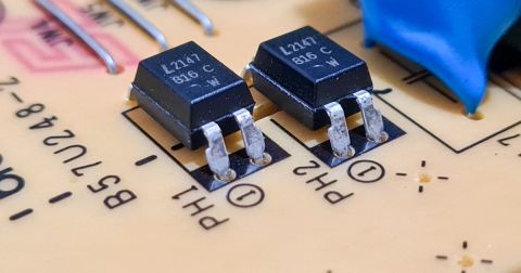
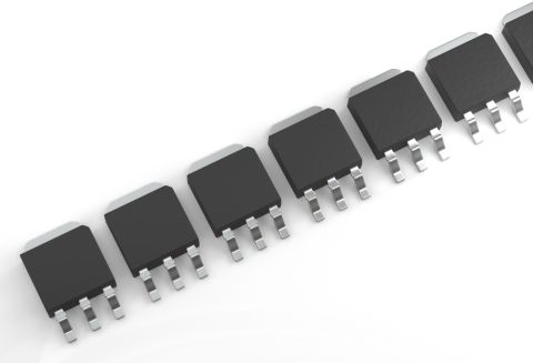
TVS diode protection circuits are some of the most common in non-industrial, low voltage settings Compared to other ESD protection components that are embedded in power management ICs or microcontrollers, TVS surge diode protectors can provide higher voltage suppression and can be placed near I/Os or any ESD source, as shown in the example below.

A typical voltage clamping diode circuit is shown below. The main responsibility of this voltage clamping circuit is to limit the accumulation of voltages on the input terminal of the buffer. Note that this could also be applied to the differential input on an op-amp. The operation of this circuit is very simple and, under normal conditions, diodes D1 and D2 are reverse biased. Whenever the voltage at the input is larger than the supply rail voltage, then diode D1 is forward biased and conducts. Similarly, when the voltage at the input falls below ground, then diode D2 is forward biased and conducts from the ground towards the input.

The above circuit could use some simple diodes with high reverse bias breakdown voltage (e.g., Zener diode), or TVS diodes that are combined in parallel or back-to-back configuration. The main factors used to determine which type of diodes are used are the breakdown voltage and forward current.
TVS diodes are categorized into two types; both types of TVS diodes are acting as opens in normal operating conditions and as short circuits to ground whenever an ESD surge occurs.
Unidirectional TVS Diodes
A unidirectional TVS surge diode for ESD protection is shown below. Note that a TVS diode does not have to be anything more than a simple Zener diode, or it could be a component marketed specifically as a TVS diode (e.g., the Transzorb series from Vishay, shown below), as is shown in the schematic below.

During the positive cycle of an ESD event, this diode becomes reverse biased and operates in the avalanche mode, resulting in an ESD current flowing from input to ground. During a negative cycle, this TVS diode becomes forward biased and conducts an ESD current. This is how a unidirectional TVS diode protects the circuit from ESD: by either preventing or allowing the flow of an ESD current, depending on its polarity.
Bidirectional TVS Diodes
The schematic below shows the typical usage of bidirectional TVS surge diodes for protecting ESD-sensitive components. Note that this is just a simple back-to-back arrangement of Zener diodes. An additional resistor could be added if additional current limiting is needed.

During the positive cycle of a transient ESD event, one of the two diodes is forward biased and the other is reversed biased, meaning one diode conducts due to its forward bias while the other one acts in the avalanche mode. In this way both diodes make a path leading to ground from an ESD source. During a negative ESD cycle, the diodes interchange their modes, again creating a pathway and the circuit stays protected. This circuit is preferable in the case where you don’t necessarily know what the possible polarity of an ESD event will be as seen from the system I/O.
Other ESD Suppressor Components
There are other ESD suppressor and transient voltage suppression components available, such as multilayer varistors, gas discharge tubes, and polymer-based suppressors. ESD suppression components are used to reduce ESD voltages below a certain limit such that a circuit or group of components is protected. A suppressor component or circuit is connected in parallel to a vulnerable line, which maintains low ESD voltage up to a certain limit and shunts the major ESD current to ground. These components often have an associated application circuit you’ll find in a datasheet, and these example circuits might include a TVS diode to provide additional low-voltage ESD suppression.
Example: Gas Discharge Tube + TVS Diode
One strategy for dealing with high voltage transient events is to use a gas discharge tube in parallel with a TVS diode, a series inductor, and a fuse. This strategy fast ESD events, slow surges, switching, and even lightning. An additional fuese is present for overcurrent protection. Gas discharge tubes are meant to deal with large transient voltages that might not originate from ESD events, but instead originate from slower sources like power surges, lightning, and switching. An image of a gas discharge tube is shown below.

The inductor and the TVS diode act like a low-pass RL circuit that provides additional filtering and slows down the rise time of the ESD pulse before it reaches the protected circuit. Once the TVS diode transitions to being conductive, the circuit will divert the current provided by the ESD pulse so that it does not impact the protected circuit. The GDT offers additional protection if there is also a risk of power surges, such as from an unregulated supply or from AC mains.

ESD Protection in Your PCB Layout
Even if you add ESD protection circuits to your design during schematic capture, it’s still important to use some smart layout choices to ensure ESD protection for sensitive circuits in the PCB layout. The whole purpose of ESD suppression is to make the circuit more reliable while reducing the cost for debugging and troubleshooting later.
- Use a ground plane in the PCB stackup: Using a ground plane inside the PCB provides a large grounded conductor that can accept any currents induced from an ESD event. It provides many other benefits such as eliminating ground loops, defines clear impedance, and provides shielding against EMI.
- Reduce the length of long routes: If routes are separated from ground and are too long, they can have high inductance. Not only can they easily receive EMI, they can experience a transient oscillation when a high voltage spike propagates through the trace. This oscillation can cause a TVS diode or other suppressor to fail to function.
- Don’t route sensitive tracks or components near high voltage nets: It’s a fairly simple concept that the probability of an ESD event is greater when a component is placed closer to a high voltage net or component. If you have components that can’t survive a large ESD event or power surge, the component should be kept away from such voltage sources. Some grounded shielding around ESD-sensitive components will provide additional protection.
- Take advantage of your enclosure: If you’re using a grounded metal enclosure, you can take advantage of the fact that it acts like a safety ground. Providing a low impedance connection from an ESD-sensitive area of the design (like a connector) back to the enclosure is one way to provide additional ESD protection.
Regarding the last point above, it’s difficult to balance the need to prevent common-mode noise with the need for shielding against ESD. Not all designs will need ESD protection in the form of a connection to the enclosure; you need to consider the environment where the design will be deployed and the magnitude of ESD that might be induced in the component.
Guaranteeing that an electronic assembly is ESD protected is very important for assemblies having external interfaces to communicate with the outer world. Although some integrated circuits will include ESD protection on the die, it’s still recommended to strategically place ESD protection circuits if the operating environment for the device creates a danger of strong ESD. This might be required in order for your device to receive FCC or CE certifications so that you can sell your product in the open market.
Whether you need to build reliable power electronics or advanced digital systems, Altium Develop unites every discipline into one collaborative force. Free from silos. Free from limits. It’s where engineers, designers, and innovators work as one to co-create without constraints. Experience Altium Develop today!

About Author
Related Resources
Related Technical Documentation
Table of Contents
Design to Release, Without the Friction
- Keep reviews tied to the right version
- Reduce handoff confusion and rework
- Spot sourcing and release risk earlier
- Work solo, share when needed
Get Started
Thank you, you are now subscribed to updates.