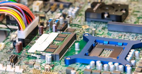


Quantum EDA Tools Are Coming for Your Circuit Board

At a Glance
Discover quantum-enhanced EDA tools. Explore millions of circuit configs in parallel, accelerating design, optimization, and simulation beyond classical limits.


What if your EDA tools could explore millions of circuit configurations at once, surfacing breakthroughs in minutes instead of weeks? That’s the promise of quantum-enhanced design. As quantum computing transitions from theoretical promise to practical tools, it’s beginning to transform how we optimize circuits.
Traditional EDA tools tackle one design iteration at a time. Quantum systems work differently: they evaluate vast solution spaces in parallel, making it possible to solve problems that were once too complex or time-consuming to explore. Engineers are already using these tools to accelerate analog optimization, model new materials, and simulate systems far beyond the reach of classical methods.
Quantum Optimization in Circuit Design
Quantum-enhanced optimization goes beyond individual component design. These tools excel at solving complex puzzles, including combinatorial problems, to improve analog circuit performance. The quantum algorithms can quickly work through millions of possible configurations, so you get better designs in less time.
In November 2024, NVIDIA announced a collaboration with Google Quantum AI at SC24 (The International Conference for High Performance Computing, Networking, Storage and Analysis). This partnership leverages the CUDA-Q platform to advance quantum processor design through large-scale simulations. Using NVIDIA Eos supercomputers packed with 1,024 H100 Tensor Core GPUs, the platform created simulations of up to 40 qubit devices, among the largest ever done. This solution reduced computation time from weeks to minutes—a major advance in scaling quantum hardware while addressing noise.
Researchers from Google Quantum AI and DeepMind also developed AlphaQubit – an AI-powered neural network decoder based on the Transformer architecture – to address quantum error correction. Tested on Google’s Sycamore quantum processor, AlphaQubit reduced errors by 6% compared to tensor network methods and demonstrated adaptability to real-world noise through a two-stage training process (synthetic data pre-training + experimental data fine-tuning). This collaboration highlights machine learning’s growing role in advancing fault-tolerant quantum computing.
In addition, Keysight and Google Quantum AI have created a new design tool called Quantum Circuit Simulation (Quantum Ckt Sim) that’s already proving valuable in quantum circuit development. Adding frequency-domain flux quantization to their simulation tools has improved how superconducting quantum circuits are modeled. The new tool, detailed in a technical paper co-authored with Google AI, offers an extensive library of quantum devices and enhanced control features to improve the accuracy and efficiency of quantum R&D workflows.
How Quantum-Enhanced EDA Works
Quantum-enhanced EDA applies the principles of quantum mechanics to process design problems more efficiently. Traditional EDA tools evaluate design options one after another, while quantum systems leverage quantum superposition to explore multiple possibilities at the same time.
Three core approaches enable quantum-enhanced EDA:
- Gate-based quantum computers, which offer flexible programming models
- Quantum annealing systems, optimized for solving large-scale combinatorial problems
- Hybrid quantum-classical algorithms that balance the strengths of both
The Quantum-Classical Interface
Electronics engineers using quantum-enhanced EDA tools must consider how the gap between quantum and classical computing is bridged. Quantum processors require sophisticated control electronics that operate at near absolute zero temperatures – typically 10-15 millikelvin (mK) for superconducting systems. This creates unique design constraints that ripple through the entire toolchain.
The interface requires precise timing control, with sub-nanosecond precision for manipulating quantum states. Modern systems use specialized cryogenic CMOS circuits operating at 4 K (kelvins) and are engineered to maintain performance while minimizing thermal load. Because of this, power management becomes critical, as even small thermal variations can disrupt quantum operations.
Implementation and Integration
Implementing quantum-enhanced EDA tools requires thoroughly analyzing how they fit into your existing design flows. In many cases, quantum processing may run on specialized hardware systems or cloud services, but engineers must still pre-process design problems using classical computing resources before submitting them to quantum tools.
A key to successful implementation lies in choosing the right problems to tackle with quantum methods. Some design tasks, such as refining analog circuit designs or placement-and-routing issues, are particularly well-suited to quantum approaches today. Traditional methods will continue to handle many other tasks more efficiently for some time.
Recent developments in implementing and integrating quantum technologies include:
- Cloud-based quantum services for experimentation: Some leading technology companies, like NVIDIA, now offer access to quantum hardware and simulators, allowing engineers to test quantum algorithms without investing in specialized equipment.
- Quantum-inspired algorithms on classical hardware: Researchers are developing classical algorithms that mimic quantum principles, providing some of the benefits of quantum computing on existing hardware.
Cost-Benefit Considerations
The investment in quantum-enhanced EDA capabilities needs to be weighed against tangible outcomes. Recent research shows that quantum methods are already delivering promising ROI in key optimization tasks, with simulation times reduced from weeks to days and measurable improvements in device performance.
While the technology is still evolving, the most successful implementations focus on specific, well-defined design challenges where quantum provides a clear advantage. Teams that start small and target the right use cases are seeing the greatest returns.
Emerging Frontiers
As quantum computing technology evolves, we’ll see increasingly sophisticated applications available for electronic design. In semiconductor R&D, quantum simulations of new materials and device physics will accelerate the pace of chip innovation. Future quantum-enhanced tools may be able to automatically generate and optimize novel circuit topologies, suggesting designs that most human engineers might never even consider.
Integrating quantum computing with artificial intelligence techniques will enable even more futuristic possibilities. AI-driven, quantum-enhanced tools have the potential to become active design partners, helping engineers explore unprecedented design spaces and develop solutions that push past conventional design limits.
Entry Points for Engineers
For engineers looking to explore quantum-enhanced EDA, several practical entry points are already available:
- Use cloud-based quantum services to experiment with circuit models and quantum algorithms, such as Amazon Braket, which provides access to hardware from IonQ, Rigetti and others.
- Explore quantum-inspired optimization techniques using familiar tools and languages via platforms like Microsoft Azure Quantum, which supports a range of hybrid and classical simulators.
- Start building quantum-aware hardware designs with development environments like IBM’s Qiskit Metal, which integrates with familiar EDA design tools and supports Python-based customization.
These examples show how major tech companies are actively investing in resources for engineers, including tutorials, simulators, and cloud platforms that support both quantum-inspired and true quantum workflows.
Quantum Skills for Electronics Engineers
A growing demand for professionals with quantum computing expertise is just around the corner. Engineers with the following skills will have a strong foundation to build on:
- Microwave engineering for 4-8 GHz qubit control
- Low-temperature ASIC design principles
- Quantum-aware EDA tool flows
- Fault-tolerant architecture co-design
Leading educational institutions are partnering with top tech companies to develop quantum engineering pathways that build on traditional electronics expertise. These programs blend quantum device physics with practical circuit design, bridging classical and quantum domains.
Next-Gen Tools for Next-Gen Engineers
Integrating quantum computing into electronic design automation will radically change how engineers approach circuit design. While the technology is still maturing, its potential to accelerate and expand the design process is already clear. Engineers who start exploring quantum-enhanced EDA today will be well-positioned to lead the next wave of electronic design innovation.

About Author
Related Resources
Related Technical Documentation
Table of Contents
Design to Release, Without the Friction
- Keep reviews tied to the right version
- Reduce handoff confusion and rework
- Spot sourcing and release risk earlier
- Work solo, share when needed
Get Started
Thank you, you are now subscribed to updates.

