


Filter Transfer Function and Pole-Zero Analysis in Altium Designer


I remember spending hours on circuit analysis problems in my electronics classes, and I learned to analyze all sorts of filter/amplifier configurations by hand. The circuits were usually tractable with Ohm’s law and Kirchoff’s laws, as long as there was no feedback in the circuit. Circuits for advanced applications, such as wideband or multiband matching circuits for RF components, can quickly become difficult to analyze by hand.
But as the number of resonant frequencies in a complex filter exceeds 2 or 3, the problem can quickly become intractable. At this point, the problem usually involves decomposition or direct solution of a 3rd degree or higher polynomial, which becomes unmanageable by hand. Even as a math guy, I’m no fan of higher degree polynomial problems. Fortunately, when dealing with complex filters, you can determine many aspects of signal behavior
Analyzing a Complex Filter Circuit
The circuit shown in the schematic below is a rather complex filter. While you may not encounter this type of filter in general practice, you’ll come pretty close when you’re designing a matching circuit for a multiband antenna. In this circuit, the source (V2) sends a signal into a bandpass filter, and the output from this portion (the voltage across the capacitor) is input into the bandstop filter. The output voltage from the filter is measured across L3 and C3. This filter circuit was built using the generic components in the Miscellaneous Devices.IntLib library. The sinusoidal source (V2) can be found in the Simulation Sources.IntLib library.

A simple analysis of this filter would say that there are two important poles; a peak in the output voltage at the bandpass RLC resonance frequency, and a zero in the output voltage at the bandstop resonance frequency. In reality, this is not correct. This is because capacitor C1 and inductor L1 also participate in resonance with the band-stop portion of this circuit, creating a complicated resonance structure in the circuit’s transfer function.
As we will see, there are more than two peaks and zeroes in the filter transfer function. This is normally done by converting the circuit and the input signal into the Laplace domain. In general, the transfer function can be written as a fraction of products, as shown in the equation below.

In this equation, each z is a zero in the transfer function, corresponding to some frequency and decay rate where the circuit is not allowed to pass an output voltage. Each p is a pole, which corresponds to a peak in the transfer function. In linear circuits without feedback, poles will appear in imaginary conjugate pairs or as fully complex conjugate pairs with negative real part. The real part of a pole will tell you the transient behavior in the circuit.
If you try to calculate the resonances by calculating critical points in the output voltage, you’ll find that you need to solve a sixth-degree polynomial for the frequencies to determine the critical points. For the circuit above, you’ll still have to solve a sixth-degree polynomial to determine the poles in this circuit. While this problem is technically solvable, it’s faster to use a SPICE simulator to determine the circuit’s behavior in the frequency domain. Instead of doing this exercise by hand, we’ll solve this problem with a SPICE simulation in Altium Designer.
Calculating the Filter Transfer Function
To calculate the transfer function for this circuit, I’ve placed two probes (I and V) at the input and output. The input current will just experience some attenuation or amplification whenever the circuit resonates at its bandpass or bandstop resonances. A comparison of the output voltage measurement (V probe) is compared with the input voltage at a specific frequency to construct a transfer function (see the above equation).
To get started, open the Simulation Dashboard, and select the sources and measurement probes to be used in the analysis.
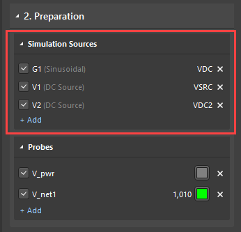
Next, enable the following analyses:
- Transfer Function: Select a source name and reference node to use for transfer function calculations in your circuit network.
- Pole-Zero Analysis: Set the input node to the net with R1 (NetR1_2) and the output node (NetC2_1). Make sure to leave the reference node options set to “0” as this will take voltage measurements with respect to ground. Note that, if there were a component somewhere on the net connected to ground, then you would need to change these options. My settings are shown in the image below. Take a look at this article for more information on interpreting pole-zero analysis results.

Filter transfer functions are usually shown in a Bode plot. Note that you can extract the transfer function directly, or you can extract the complex transfer function from an AC sweep. A Bode plot is convenient as it shows the magnitude and phase of the transfer function in the frequency domain and in the steady state (after all transients have decayed); this allows you to see how the filter affects both important aspects of input signal behavior in a pair of plots.
Analyzing Your Filter Transfer Function Results
Once you’ve finished the above setup, you’re ready to run your simulation. Hit F9 on the keyboard or click Simulate → Run Simulation. You’ll see a number of plots in the AC sweep results, and a separate window will appear, which shows the pole-zero analysis results. The circuit above contains 6 poles and 2 zeroes. These are shown in the image below. Note that the units on each axis are in units of angular frequency (rad/s). If you want to examine the behavior in the AC sweep results, then you need to convert to frequency values.
Two of the poles lie along the negative portion of the real axis (i.e., they have no imaginary part). These values show that you can place a momentary output from the circuit when sourcing with a step function or impulse. However, the output will quickly decay with two superimposed exponential decay rates. The other poles and the two zeros correspond to specific frequencies, the behavior of which can be seen in the AC sweep results.

The graphs below show the behavior of this circuit in the frequency domain. The zero at 1.453 MHz and the poles at 800.7 kHz and 2.885 MHz are clearly visible in the Bode plot (blue curve in the top graph). The bottom graph shows the phase of the transfer function, however, the zeroes can’t be seen in the output voltage plot (overlaid in the top graph, purple curve). The output voltage graph shows that poles 3 and 4 have gain of ~2.3, and poles 5 and 6 have gain of ~6.

More With Transient Analysis
If you want to go further with this simulation, you can set the input frequency to any of the values for the poles shown in the Bode plot and run a transient analysis. This circuit shows some interesting transient behavior due to the complex resonant behavior for the two portions of this filter circuit.
You can also see how the transient responses in the input current and the voltage/power delivered to the capacitor differ over time. An example is shown below. An important point to remember here is that this is an LTI circuit: the impedance does not vary in time, so the transient response seen here is standard behavior in a linear system. From this plot, we see that the voltage (and reactive power) delivered to the capacitive load will slowly increase due to the overall reactive nature of this filter circuit. We could certainly look at other voltages/currents at different points in the circuit to see how this initial rising behavior in the input current occurs. I'll leave this as an exercise for the reader.

The pre-layout analysis tools in Altium Designer® let you do more than just analyze filter transfer functions for linear circuits. You can examine noise immunity, transient behavior, temperature effects in your circuits, and much more. You can then capture your schematic as an initial layout and design all aspects of your next PCB. You’ll also have a complete set of tools for documenting all aspects of your project, managing your supply chain, and preparing deliverables for your manufacturer.
Now you can download a free trial of Altium Designer and learn more about the industry’s best layout, simulation, and production planning tools. Talk to an Altium expert today to learn more.

About Author
Related Resources
Related Technical Documentation
Table of Contents
Design to Release, Without the Friction
- Keep reviews tied to the right version
- Reduce handoff confusion and rework
- Spot sourcing and release risk earlier
- Work solo, share when needed
Get Started
Thank you, you are now subscribed to updates.

