


Can You Use Series and Parallel Termination on the Same Net?


Series and parallel termination are the most common resistive termination options for digital signaling. The reason is that resistance is a wideband quantity and does not start to be affected by parasitics until well into the GHz range. At the channel bandwidth associated with most digital signals, there are cases where an unterminated line actually needs termination, even if there is no impedance specification in the interface.
As both options are viable for digital signals, which of these should you use to terminate a long transmission line with no impedance specification? There is sometimes a perception that both should be used, or that both can be used on every net. There are cases where both can be used at the same time, but typically only one is chosen as it can eliminate the need for the other.
In this article, I'll look at the signaling involved in both series and parallel terminations, and the specialty case where you might see both terminations.
Series and Parallel Terminations Via Transfer Functions
The explanation given below is not going to be based on signal dynamics per se. For that, you can read this good article from Kella Knack which shows example waveforms. Instead, I'll look from the transfer function perspective to show exactly what happens to voltage levels in a transmission line. This also reveals the effect of bandwidth on digital signals.
What I will show below regarding these two terminations and why they are often not used together on the same net is based on the following assumptions:
- The interfaces have no specified impedance target, meaning the trace impedance could be anything
- Driver impedance is generally a low value, and load impedance is modeled as a simple load capacitance
- The driver output impedance is known or can be determined, such as from measurement or simulation (IBIS)
Now let's look at each of these terminations in detail.
Series Termination Transfer Function
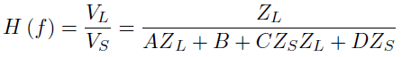
The circuit shown below illustrates the formalism used to determine transmission line transfer function from ABCD parameters. Note that we could also use S-parameters, but ABCD parameters are much easier.

The transfer function is the ratio of the load voltage to the source voltage. The great thing about a transfer function approach is that the load voltage is explicitly defined in terms of the source impedance as shown above. Now we can substitute in our source impedances and any series resistance.
When the series resistor is used to perfectly terminate the transmission line, the resistor is sized to be R = ZS - Z0. This resistor is normally placed at the driver IO pin, and we now have the relation where the total source impedance is ZS = Z0 as this is the new total output impedance. Using the definition of ABCD parameters for a transmission line, we have:

Here, we have a transfer function that looks like a voltage divider involving the load impedance and the transmission line impedance. The voltage at the load is:

If we take the load impedance and make it very large, we would have the following value for the voltage at the load:

This applies within the channel bandwidth as defined by the load capacitance. How does the signal from the driver become affected after interacting with the total source impedance, which includes the series resistor? If you use the definition of ABCD parameters and calculate V1, you get the following if ZS + R = Z0:

Now we see the function of the series resistor: when perfectly matched, The source impedance and trace impedance act like a voltage divider. If the source impedance is below or above the trace impedance, we would observe overshoot or undershoot after reflection off the load.
It is only through reflection off the load that the halved signal level is restored to the full level. This is why we would not also typically apply parallel termination on the same net when the receiver voltage must see the same value as the source voltage. Now let’s look at parallel termination on its own.
Parallel Termination
With parallel termination, the entire point is to suppress the reflection off the receiver, as I mentioned above. In an impedance-specified bus, termination is usually placed on the semiconductor die. In a more general case, such as with certain line drivers, the impedance is not specified and so termination might need to be applied manually.
Parallel termination with no series resistor termination works as follows:
- Because there is no series resistor, the voltage division function causes the entire signal to be placed on the transmission line (V1 = VS)
- The signal then propagates to the load and does not reflect, so it is totally absorbed across the parallel resistor
If we assume a perfect source impedance of ZS = 0, the transfer function for parallel termination gives the following relationship for the load and source voltages:

With parallel termination, we see that there is a factor 2 in the numerator. The termination circuit creates a resistance in parallel with a load capacitance, where the resistance is R = Z0. Within the channel’s knee frequency bandwidth limit as defined by that capacitive load, the load impedance is very nearly equal to the parallel resistance. This again gives us the voltage seen at the load when R = Z0 and thus ZL = Z0:

Once again, we get back to the full strength signal that we sent into the interconnect.
If the source impedance is non-zero, go back into the transfer function definition and plug in the value for your source impedance. This could be extracted from measurements or from simulations.
Can You Use Both Series and Parallel Termination?
When we compare the general form of the series termination resistor transfer function, it should be very clear why we don't intentionally also place a parallel resistor when there is already a series resistor. If you perfectly match with a discrete series resistor, and then also match with a parallel resistor, then only half of the signal level makes it onto the line and this is absorbed by the parallel resistor. In other words, the voltage seen at the load is:

If you are using a component with a 3.3 V signal level and the receiver also demands a 3.3 V signal level, then you might not be able to use both series and parallel termination at the same time. You would have to look carefully at the logic thresholds in the receiver to make sure the voltage at the load is not too low.
The corner case is where you intend to step down from a source voltage to a lower load voltage. For example, with a 3.3 V source and a load that needs 1.8 V amplitude, the signal level received at the load would be 1.65 V with both series and parallel termination. This might be at the bottom end of the voltage required to register as a HIGH logic state in the receiver. We can find other examples of common logic levels where we get the same result.
Instead of trying to engineer a step down with termination resistors, normally you would change between two different signal levels using a level shifter. These components are designed to support both specific interfaces or they can be compatible with a range of possible interfaces. These components will accept different supply voltages and will create a replica of the incoming signal at the output, but at a higher or lower voltage. An example for the SN65DP159 from Texas Instruments is shown below.

Does All This Apply to Differential Pairs?
The answer is "yes" with an asterisk; if using a differential pair then replace the characteristic impedance in the above transfer functions with the odd-mode impedance, and calculate the difference in the opposite-polarity signals at the receiver side of the interconnect.
Most differential interfaces have specific termination requirements and trace impedance requirements, which is already implemented on-die at the driver side of the line (at minimum). When DC coupling is required, that on-die termination at the driver side precludes the use of a series resistor. In other instances, parallel termination could be used when the receiver component does not have on-die termination, which is not common. The use of termination (series, parallel, or both) can still be applied in specialty cases, but it would be specified in datasheets, determined through testing, or it would already be included on-die.
Once you’ve found the transmission line transfer function and you’re ready to layout your channel, use the design and layout tools in Altium Designer®. To implement collaboration in today’s cross-disciplinary environment, innovative companies are using the Altium 365™ platform to easily share design data and put projects into manufacturing.
We have only scratched the surface of what’s possible with Altium Designer on Altium 365. Start your free trial of Altium Designer + Altium 365 today.

About Author
Related Resources
Related Technical Documentation
Table of Contents
Design to Release, Without the Friction
- Keep reviews tied to the right version
- Reduce handoff confusion and rework
- Spot sourcing and release risk earlier
- Work solo, share when needed
Get Started
Thank you, you are now subscribed to updates.

