SAP (Semi-Additive Process) PCB Design with Flexible Circuits


In a previous blog, I issued a challenge to the PCB designer community. How creative can you be when starting to think through a printed circuit board layout knowing that you now have the ability to design with 25-micron line and space, a significant density improvement over the traditional 75-micron trace and space, which has been a long-time limitation of the subtractive etching process for PCB fabricators.
One interesting and creative approach that we see is designing with the intention of using gold as the conductive metal rather than copper. If you are not familiar with the A-SAP™ process, which is Averatek’s Semi-Added Process for PCB designs, this process begins by etching away all copper from the base laminate. Once all copper is removed, the fabricator then builds back the conductor pattern. Not only does this semi-additive process enable much finer feature sizes, once the copper is etched away, it can also be used to create traces from metals other than copper.
With flexible materials, a combination of metals and dielectrics that is gaining popularity is the use of either polymide or LCP (Liquid Crystal Polymer) as the dielectric and gold and/ or platinum as the conductive metal. This provides a much more biocompatible solution for medical applications that requires the circuitry to interact with the patient’s body.
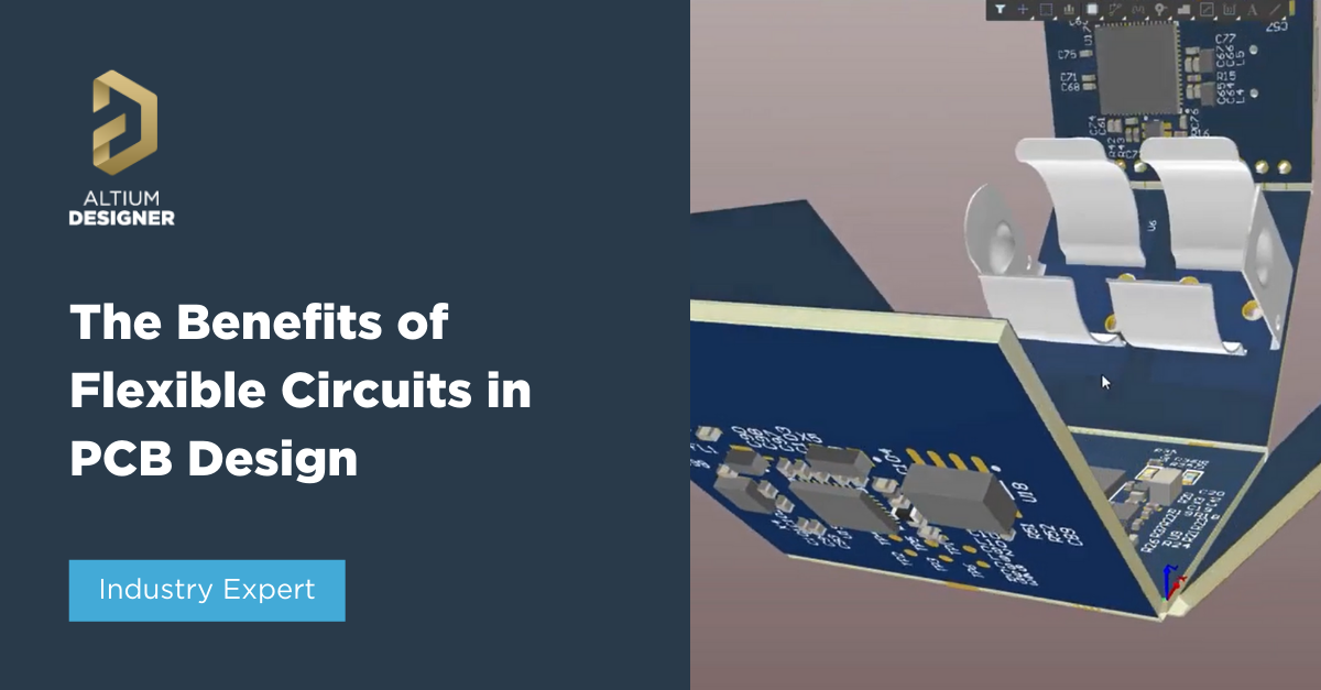
To spark some creative thinking, imagine the benefits of this improved circuit density, allowing much smaller package sizes. Flexible circuits and rigid flex circuit construction are often used in medical applications to reduce the size and weight of the electronics in medical devices. Everything from portable medical equipment to insulin pumps to cauterizers have been evolving to printed circuit designs with flexible materials. The ability to form smaller packages, bend and wrap around corners and the lighter weight of these materials make flexible circuit designs a top candidate to solve challenges in space and weight.
Now, with the adoption of semi-additive processes, both A-SAP™ and mSAP technologies, much finer lines and spaces are possible on flexible materials, further leveraging the benefits of these flexible materials for space and weight improvements. Intuitively there are many ways this can be leveraged as an additional e. Clearly, the overall size of the flexible circuit can be reduced when the traces and spaces are reduced from 75 micron to 25 micron. Often, the overall number of layers can be reduced with this high-density routing technique. Looking at things from another perspective, additional electronic functionality can be added to an existing footprint. It is also important to mention that not all layers need to be SAP PCB layers, this technology is specific to layers and can be used with subtractive etch layers for larger features and ground planes. It is also important to note that these processes don’t have to be 25 microns, that is simply a frame of reference for what is capable today. The feature sizes will be dependent on your fabricators photoimaging capabilities and will vary from fabricator to fabricator.
These semi-additive PCB fabrication processes can also be used with rigid flex construction. PCB fabricators now have the ability to create these very fine features on both flexible materials and rigid materials. Why not take advantage of the ultra-high-density routing to reduce layers and ultimately the complexity of the rigid flex design? This is especially impactful to pricing and complexity when comparing a rigid design to a flex or rigid flex design where the cost per layer is typically higher than purely rigid constructions. Reducing layers in a rigid flex construction and simplifying a complex design can have a significant impact on yield, lead-time and cost.
One note of caution, please be sure to be mindful of your printed circuit board fabricator’s capabilities. As we have discussed in previous blogs, not all fabricators have the same capabilities, especially when it comes to flexible circuits and rigid flex designs. If your fabricator is not experienced in working with flexible materials and rigid flex construction processes, simply adding the capability to create these high-density layers will not change that. Search for a fabricator that is currently successfully and repeatably producing flex and rigid flex with the subtractive etch process and then narrow that to the fabricators in your list that have added the mSAP or A-SAP™ process for their designs.
If you are interested in exploring the concept of using gold rather than copper as the conductive metal, that is something that is new to most. There is a small group of PCB fabricators doing this now and others that will be implementing this as the market demand grows. This technology is being used in neural probe applications with published data, along with other implantable and insertable applications in the medical field.
As always, please continue to reach out with your questions and creative ideas for how to best apply the benefits of these semi-additive process capabilities to solve your pressing printed circuit board design challenges!
Would you like to learn more about how Altium Designer® can help you with your next PCB design? Talk to an expert at Altium.


