


Stack-Up to Success: Avoid the Pitfalls

At a Glance
Avoid warpage, impedance issues, and delays. Learn how smart PCB stack-up design ensures performance, reliability, and smooth fabrication.


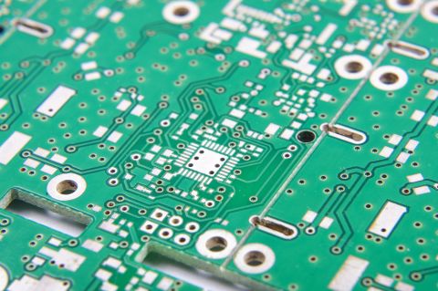
We’ve all been there, you submit what looks like a solid design, only to run into questions about material substitutions, unexpected impedance calculation results, or a worst-case scenario, a PCB that comes back from the fabricator warped beyond usability. While there are many variables that impact yield and reliability, your PCB stack-up is often the unsung hero, or the hidden culprit.
For PCB designers working on high-density, high-speed, flex, or rigid-flex builds, your stack-up is more than just a list of layers. It’s a roadmap that drives signal performance, thermal management, manufacturability, and mechanical stability. So, let’s walk through the most common stack-up pitfalls and more importantly, how to avoid them.
Why Your Stack-Up Deserves More Attention
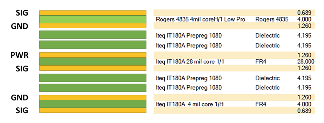
Think of the stack-up as the architectural blueprint for your board. It defines everything from impedance profiles to how copper is distributed across layers. It also sets the tone for what materials will be used, how many lamination cycles are required, and how well your board will hold up to thermal and mechanical stresses.
Get it right, and your board performs beautifully. Get it wrong, and even the most elegant circuit design can end in frustration.
Pitfall: Unbalanced Stack-Ups and Warpage Risk
One of the most common issues we see in fabrication is PCB warpage. Especially in rigid-flex designs or multilayer ultra-HDI builds, an unbalanced stack-up, where copper distribution or dielectric thicknesses are uneven from top to bottom, can cause real headaches.
When layers heat during lamination or reflow, differential expansion kicks in. If the structure isn’t symmetrical, the board can bow, twist, or delaminate.
Avoid it: Aim for symmetrical layer pairing, especially in boards with four or more layers. If layer symmetry isn’t possible due to constraints like component density, talk to your fabricator about compensation strategies like copper balancing or using counterweight materials.
Pitfall: Over-Spec’ing or Under-Spec’ing Materials
Specifying materials is often where designers either overdo it or don’t say enough. Calling out a specific dielectric that’s hard to source, or forgetting to specify a controlled impedance layer, can both slow down your build.
Material choices influence everything from Dk/Df values and impedance to how thin your stack-up can be. And in flex and rigid-flex designs, material flexibility, adhesive content, and thermal stability are critical.
Avoid it: Know which layers are performance-critical and clearly define what matters most: dielectric constant, thickness, loss tangent, or flexibility. Be specific where you need to be, and open to alternatives where performance allows. Your fab partner may suggest in-stock substitutes that save time and cost.
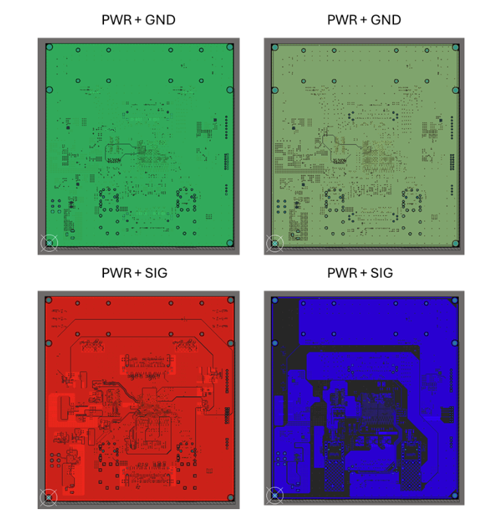
Pitfall: Ignoring Copper Distribution
Uneven copper distribution across layers isn’t just a cosmetic issue, it can affect impedance, plating uniformity, and the thermal profile of your board. Inconsistent copper causes etching challenges and can lead to local warpage or rough surface finishes.
Avoid it: Balance copper as evenly as possible between layer pairs. Use dummy fills if needed to match adjacent planes or signal layers. And remember while copper pours are helpful, they still need proper spacing, clearances, and thermals to avoid creating new problems.
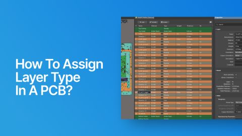
Pitfall: Poor Communication in Documentation
Even if your stack-up is thoroughly thought out, it doesn’t do much good if the fabricator can’t read your intent. I’ve seen stack-ups missing layer descriptions, unclear core/prepreg notes, or inconsistent impedance targets that require back-and-forth clarification.
Avoid it: Provide a clearly labeled stack-up diagram with all dielectric thicknesses, copper weights, and materials. If impedance control is required, call out the layers involved, the target value, and the allowable tolerance. If there’s flexibility in materials, say so.
Your documentation doesn’t need to be fancy, it just needs to be clear.
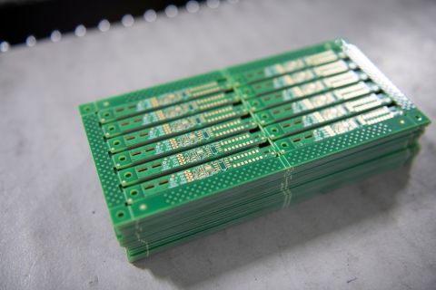
Pitfall: Forgetting the Fabrication Process
Designers sometimes create stack-ups that look great in theory, but they’re missing a critical piece: how the board will actually be built. Ultra-HDI stack-ups using SAP or mSAP, for example, need ultra-thin copper layers and laser-drillable dielectrics. Flex circuits need to account for bend areas, adhesive layers, and potential ZIF connectors.
Avoid it: Consider the fabrication process as part of the stack-up plan. If your board requires sequential lamination, make sure layer sequencing reflects it. If it includes buried or stacked vias, note that clearly and account for the aspect ratios and drill constraints.
The earlier you bring your fab partner into this conversation, the better.
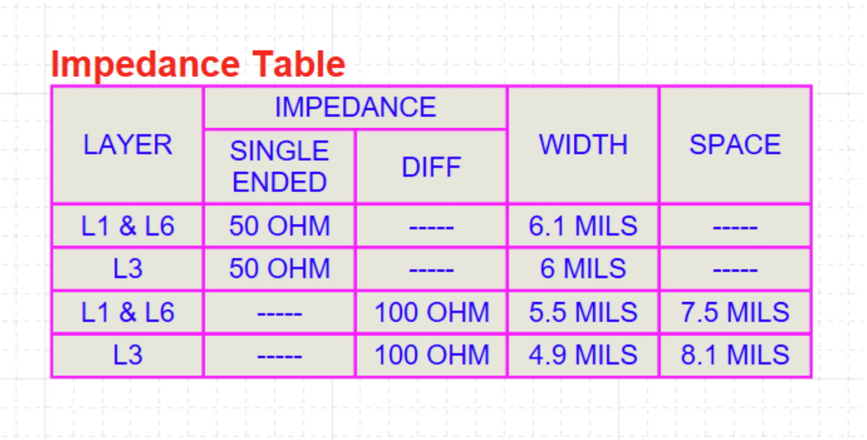
Pitfall: No Impedance Targets (or Way Too Many)
Controlled impedance doesn’t mean every trace has to hit a specific number. But I’ve seen both extremes—designs with zero impedance callouts, and designs that list every differential pair with unrealistic tolerances.
Avoid it: Do a back-of-the-envelope calculation to see what your trace widths will be for different impedance values and layers, which will ensure your stackup spec will not force traces that are too large or too small. Then, call out impedance control where it matters: high-speed interfaces, RF sections, or clock traces. Include your target (e.g., 50Ω single-ended, 100Ω differential) and a tolerance (+/-10% is standard unless you really need tighter).
Work with your fabricator to tune stack-up parameters for those critical layers. They’ll simulate it and suggest changes to trace width or dielectric thickness if needed.
Final Thoughts
Your stack-up isn’t just a list of layers, it’s a design decision that ripples through fabrication, assembly, and performance. In today’s advanced printed circuit board technology, especially with UHDI, flex, and hybrid builds, smart stack-up planning is a competitive advantage.
Start early. Collaborate often. Make your documentation clear and your priorities obvious. You’ll spend less time chasing down material questions and more time getting your design to market.
And if you’re ever unsure, reach out. Your fabrication partner is your best ally when it comes to translating your design vision into a reliable, manufacturable board.
About Author
Related Resources
Related Technical Documentation
Table of Contents
- Why Your Stack-Up Deserves More Attention
- Pitfall: Unbalanced Stack-Ups and Warpage Risk
- Pitfall: Over-Spec’ing or Under-Spec’ing Materials
- Pitfall: Ignoring Copper Distribution
- Pitfall: Poor Communication in Documentation
- Pitfall: Forgetting the Fabrication Process
- Pitfall: No Impedance Targets (or Way Too Many)
- Final Thoughts
Design to Release, Without the Friction
- Keep reviews tied to the right version
- Reduce handoff confusion and rework
- Spot sourcing and release risk earlier
- Work solo, share when needed
Get Started
Thank you, you are now subscribed to updates.