


Material and Process Considerations That Influence Performance

At a Glance
Stack-up choices shape PCB performance, reliability, and manufacturability, especially in flex and UHDI. Learn how to design with materials in mind.


PCB stack-up decisions might not be the most glamorous part of the design process, but they’re one of the most telling. If you want your board to perform reliably, pass inspection, and make it through manufacturing without costly surprises, the stack-up is where you begin. And if you're working on advanced technologies like flexible circuits or Ultra HDI, your stack-up provides strong information about performance, reliability, and buildability.
Let’s look at how stack-up choices influence the entire fabrication and assembly process and what designers should keep in mind when working with flex or UHDI designs.
Stack-Up: The Foundation of Functionality
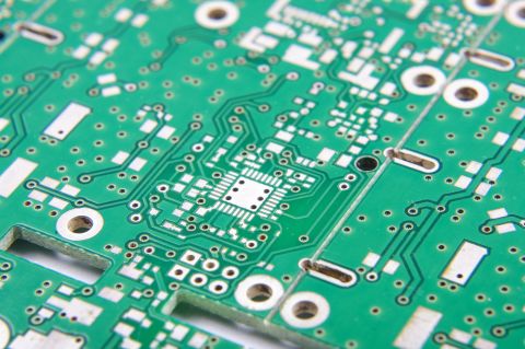
From signal integrity and impedance control to thermal performance and manufacturability, your stack-up is where many of your board’s key electrical and mechanical properties are defined. It communicates copper weights, dielectric materials, thicknesses, and the order in which layers are built and bonded.
For rigid boards, a well-thought-out stack-up helps control impedance, reduces crosstalk, and supports consistent plating and lamination. For flex and rigid-flex boards, it’s even more critical, as the materials are thinner, more sensitive to processing conditions, and more likely to be influenced by mechanical stress.
Material Matters: Diving Deeper into Flex and Ultra HDI
When it comes to flexible circuits, the choice of materials isn't just about electrical performance, it also defines how the board will behave mechanically. Polyimide remains the standard due to its flexibility, thermal stability, and chemical resistance. But within that category, there’s a growing shift toward adhesiveless constructions. These materials eliminate the need for bonding adhesive layers, reducing thickness and improving dynamic flex performance.
Another area of development is ultra-thin flex materials designed for high-speed and RF applications. These materials often come with improved dimensional stability and controlled Dk/Df values, making them ideal for impedance-controlled flex circuits used in automotive radar, aerospace, and next-gen consumer electronics.
On the Ultra HDI front, new resin systems and dielectric materials are enabling feature sizes once considered out of reach. Advanced materials like Ajinomoto Build-up Film (ABF), Shinko semi-additive laminates, and other laser-drillable ultra-thin dielectrics support trace widths down to 10 microns or less with exceptional reliability. These materials often exhibit lower dielectric constants (Dk) and dissipation factors (Df), essential for high-speed digital designs and RF applications.
Copper foil is also evolving. Traditional rolled annealed (RA) and electro-deposited (ED) copper are now joined by Very Low Profile (VLP) and reverse-treated copper foils, optimized for semi-additive and modified semi-additive processes (SAP/mSAP). These foils provide a smoother base for finer features and help improve etching uniformity.
There’s also movement toward embedded capacitance materials and nanolayer dielectrics for multilayer UHDI stack-ups. These new materials improve power integrity while reducing layer count—a huge plus in miniaturized designs.
Communicating Your Intent: More Than Just Layer Count
Don’t assume your manufacturer knows what you mean when you send over a simple layer count or rough outline. If you’re designing a rigid-flex, spell out the flex-to-rigid transitions. Indicate areas where dynamic bending will occur and what type of flex stack you expect (e.g., single-sided flex with coverlay vs. dual access flex).
In Ultra HDI designs, clearly communicate which layers require SAP or mSAP and what feature sizes are expected. Flag layers with ultra-fine traces (25–40 µm or less) and specify via types (stacked, staggered, blind, buried) early. Call out dielectric thicknesses and required tolerances. If you’re targeting HDI Class III reliability, note that too.
The more clarity you provide upfront, the smoother the fabrication process. And the fewer assumptions your manufacturer has to make, the better your yield and long-term reliability.
Don't Forget About Process Flow
Stack-up documentation is more than a design artifact. It’s a roadmap for how your board will be built. Does your board require sequential lamination? If so, how many cycles? Are there any hybrid material sets that require adjusted lamination pressures or thermal cycles?
In Ultra HDI builds, process flow becomes even more critical. SAP and mSAP methods may require specialized pre-treatment, ultra-thin copper deposition, laser ablation, and etch-back sequences. Misalignment or shrinkage can ruin your yield. Your stack-up should account for cumulative tolerances, thermal expansion, and surface prep strategies.
Flex stack-ups bring their own considerations. Are there stiffeners? Shield layers? EMI films? Will the board bend in one direction or multiple? Does it require controlled impedance or is it strictly power and low-speed signals? All of these influence the lamination sequence, tooling strategy, and inspection points.
What the Stack-Up Doesn’t Say (But Should)
Your stack-up isn’t just about layers, it’s your chance to express design intent, tolerances, and functional priorities. Consider adding notes on:
- Critical impedance layers and target tolerances
- Controlled bend areas and mechanical keep-out zones
- Acceptable material substitutions for global sourcing
- Thermal via requirements or embedded passives
- Reliability expectations (IPC Class 2 vs. Class 3, etc.)
This extra context helps your manufacturer catch potential issues early and gives them the opportunity to recommend alternative materials or processes that better align with your performance needs and cost goals.
Final Thoughts
A stack-up is more than a structural blueprint, it’s a communication tool. It tells your manufacturer what you care about, what you expect, and where you’re willing to compromise (or not).
In the world of UHDI and flex, where every micron matters and the material choices are evolving rapidly, taking the time to document and communicate your stack-up with precision is one of the best investments you can make in your design’s success.
So, don’t treat your stack-up as an afterthought. Use it as a strategic asset. Start early. Be detailed. Ask questions. And bring your fabricator into the loop. When your stack-up speaks clearly, your board is that much closer to being built exactly the way you envisioned it.
About Author
Related Resources
Related Technical Documentation
Table of Contents
Design to Release, Without the Friction
- Keep reviews tied to the right version
- Reduce handoff confusion and rework
- Spot sourcing and release risk earlier
- Work solo, share when needed
Get Started
Thank you, you are now subscribed to updates.

