Team Collaboration & PCB Design

Created: February 10, 2017
Updated: October 27, 2020
Team Collaboration & PCB Design

There was a time when once a circuit design was completed, it was handed off to “the PCB designer”, who then produced the board layout. Now, with products as complex as tablets, smartphones and even electronic games, there is no single person involved with the PCB. Products are designed by teams of experts and without the ability to effectively collaborate, time is wasted and errors introduced.

There was a time when once a concept design was completed, it was handed off to “the PCB designer”, who then produced the final PCB layout. Now, with products as complex as tablets, smartphones and even electronic games, team collaboration & PCB design is critical. Products are designed by groups of experts, and without the ability to effectively collaborate, time is wasted and errors introduced.

The process is further complicated by the fact that often the team is not all in the same location, so software tools to coordinate, document and share among the team are imperative to smooth workflow. This paper explores several questions that are often asked when evaluating PCB tools that have powerful collaboration functions:

- Is there a downside to working in a group PCB design environment in absence of a powerful collaborative PCB design tool?

- How can a PCB design tool with robust collaboration tools benefit your team?

- What collaboration features should you look for when considering your options for PCB design tools?

THE PITFALLS OF WORKING IN A COLLABORATIVE PCB DESIGN ENVIRONMENT

The number one challenge in a collaborative atmosphere without the proper tools is communication. Ineffective communication results in obstacles, delays, and failures within the design process – costing time and money. Here are four serious problems that significantly effect a collaborative design environment.

No Synchronization of Product Lifecycle Management and Design Data: Without collaboration tools, designers can inadvertently change the same part of the design, resulting in fatal data conflicts. Team members can be left with the choice of unknowingly working with obsolete versions, redoing unnecessary work or attempting to sort through the inconsistencies.

Design teams that are a bit more sophisticated and use exchange files between their MCAD and ECAD (electronic designers) in Printed Circuit Board PCB design work employ a static file transfer of the database. Although using exchange files is better than nothing, it is extremely difficult to determine what data has changed, and where changes were made and by whom. Without this information, true synchronization cannot occur and the same problems arise.

Inefficient Teamwork on the Same Design: Being able to view all the work taking place on a design is critical for efficient workflow. All engineers involved need to understand each other’s intent and vision, which requires comprehensive communication.

However, email threads, notes and other kludgy communication methods disrupt efficiency and productivity within the workflow. The process is cumbersome and information can be lost if someone isn’t cc’d on the message – and even when they get the email, they might not read it on time.

Intermittent or rare PCB layout exchange often results in issues down the road with the final product, which means designers have to retread their steps, determine the source of the violation and re-work their design. Team members are essentially doing the job twice to ensure the overall design can achieve final PCB layout and schematic capture signoff.

Communication Across Different Design Domains: While the job of the PCB designer centers on the board as just one element of the complete, final product, there are actually many people involved. Electrical and mechanical engineers and CAD technicians working on the printed circuit board shape their jobs to do, while – on the manufacturer side – there are manufacturing specialists, and logistical and supply chain experts.

Each group that touches the PCB design software uses different design domains, making it nearly impossible to communicate in the same “language” while interpreting the data in their own native application. There’s no integration of the multiple domains into a single, streamlined workflow, so multiple designers with access to the same board may impact the work of others who have access to the project - creating conflicts that result in costly, time-consuming mistakes.

Lack of Accountability: A team not working in a collaborative atmosphere during a PCB design process will be frustrated when they reach the end of the project only to find considerable conflicts. Mistakes were made due to lack of communication and failure to synchronize design data. But because there’s no way to track changes to the design and find the source of the error in a non-collaborative work setting, there’s no accountability or transparency. Worse, team members may make mistakes and may not know it. So, the errors will continue – causing additional costs and more time, impacting productivity.

BENEFITS OF PCB COLLABORATION: EFFICIENCY AND CONSISTENCY

If you’ve been working in a non-collaborative environment, many of the pitfalls are probably very familiar to you. The hassles are frustrating and squander your valuable time. In general, the benefits of team collaboration tools are increased efficiency and productivity, and consistency to eliminate the redundancy that leads to conflicts in PCB design. The specific advantages of collaboration tools further emphasize the downside of a non-collaborative workflow.

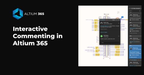
Work with Each Other, Not Against Each Other: Collaboration tools allow all team members to see the same board as it’s simultaneously worked upon by multiple designers, and view differences among different versions. Managers can use or delete changes as necessary without impacting the work of individual designers. With the proper permissions, everyone can add comments and provide feedback within a streamlined review process - all in real time.

Simplified Design Data Management Throughout the Workflow: To avoid conflicts, it’s critical that all team members are working from a single source of design data. In a fully collaborative environment, every component created and applied to a design has an “approval state” to maintain data integrity. Projects are managed within the PCB design software instead of informally through emails and notes.

Improved Comparison Management: Collaboration solutions feature design tools that can compare and detect differences among several versions of a PCB, with pinpoint accuracy. Differences are presented before the user, who can decide which changes to accept and which to decline – with just a couple clicks. Most platforms include capabilities to manage numerous differences and resolve them without creating costly conflicts that can cause delays.

Consistency Within Software Configuration: A collaborative team environment means control of PCB design tool configuration through a centralized system. All team members use tools that are subject to the same organizational standards to ensure consistency and eliminate conflicts.

Collaborate from Anywhere: A collaboration solution brings your design team together in developing boards, whether members are across the hallway or across the country. Engineers can reference designs from anywhere, designers can stay on task when traveling, and you can incorporate a remote workforce to supplement permanent employees.

Capabilities for Collaboration Outside the PCB Design Team: A unified software landscape integrates all tasks, projects and component data into a single package for a streamlined design process and great final schematic capture. PCB designers can work with other designers outside your immediate team without the challenges of multiple domains. Some Printed Circuit Board PCB design team collaboration tools feature links to suppliers, giving you real-time accuracy on pricing and quantities from the vendors you use most.

Focus on the Work, Not the Workflow: Collaborative tools manage team members communication and handle the back-end processes involved when you’re working as a team for PCB design. They also automate certain process and detect key differences that cause errors down the road. Engineering teams can concentrate more on the work and less on the workflow. With more time freed up due to fewer communication hassles, they can work on innovative, creative designing.

SIX CRITICAL FEATURES TO LOOK FOR IN PCB COLLABORATION TOOLS

You can reap the significant benefits of connected, communication-rich collaboration by implementing the right tools to suit your needs. When considering your options for Printed Circuit Board PCB collaboration tools, consider the following features to ensure positive return on investment and maximum productivity.

Live Collaboration Tools: PCB design in a team environment requires tracking of the tasks being conducted by all designers working on the board at any given time. Tools that provide you with details on the activities of other users are necessary, including who is logged into the system and who has the same board file open as their own local copy. Look for solutions that feature a centralized dashboard that logs collaborator and work region details within the same collaboration server path.

Version Control: Team collaboration on PCB design requires a version control system that allows you to:

- Easily store all project files in a central repository with back up redundancy;

- Undo changes across one or many files;

- Store and access any board from any point throughout its developmental history;

- Work independently within a collaborative setting, with local copies of the files you need - which can be uploaded to the repository when development reaches a certain stage.

Work Regions: As a designer, you can work more effectively with a PCB collaboration solution that enables you to define your own work regions. All users should be able mark out a territory on the board. For best viewing, the work regions should be easy to navigate, free of clutter, so you’re only focusing on the task at hand rather than manipulating software. In addition, it’s essential that a PCB collaboration platform allow each user to see the work regions that other designers have defined as their own space on the same board.

Handling Differences: In PCB design collaboration, you should have access to tools that allow you to seamlessly perform difference comparison. When you’re the only one working on a particular board, you need to be able to check your version against:

- One that exists in the central repository;

- An older version that exists in the central repository; or,

- One that’s stored on a hard drive or within your network.

Diff’ing and merging is a key feature you’ll need in a PCB collaboration tool. You must be able to detect and resolve differences with a sophisticated differencing engine that identifies even the slightest conflict between two boards. In a collaborative work environment, this means your PCB tool must function in two distinct ways:

A two-way comparison that displays differences between your current board and another version: what it is versus what it was.

A three-way comparison when someone else is also accessing the same board. This avoids the situation where you and a team member are working on the same board, but you want to see what your colleague has done - and possibly incorporate the changes. A three-way comparison tool enables you to compare:

- The original version you checked out from the storage repository;

- Your version, to which you’ve applied changes; and,

- Your colleague’s version.

With both two- and three-way comparison tools, displaying differences can become cluttered, resulting in errors and inconsistencies for the designer. So when considering options for PCB collaboration tools, look for solutions that display multiple versions of a board cleanly and clearly.

Merge Resolution Comparison: A PCB solution with two- and three-way comparison tools should also give you the option of merging changes into your version of the board before checking it back into the central repository. The most effective PCB design and collaboration tools will also notify you when merges are required due to another user’s activity.

Resolving Differences: In a PCB collaboration system, you should be able to resolve differences by merging those detected in the original document into the current version of the board. You can improve productivity by selecting a solution that automates this task according to your settings. Of course, you’ll need PCB design tools that also enable you to select certain changes you want to keep and those you want to bring in from another user’s work.

CONCLUSION

In current PCB design environments, engineers aren’t always in close communication with other members of their design team. Most products are developed through collaborative efforts that encompass groups that might span several countries and continents. Communication is critical in a collaborative environment. Poor communications causes errors, unresolved differences and version inconsistencies – ultimately costing time and money in the production process. Altium Designer is a PCB editor that can unify cross platform projects and design environments.

For effective collaboration, a PCB design solution must implement these five critical features:

- Allow multiple users to access the same board, to work on and save to storage - without impacting others’ tasks;

- Add traceability and accountability for all team members;

- Accurately compare files and detect differences across multiple versions of the same board;

- Resolve differences that are identified and allow the user to choose those that proceed;

- Automatically handle large difference volume and take resolution actions without creating conflicts.

 
Open as PDF

Related Resources

Related Technical Documentation

Back to Home
Thank you, you are now subscribed to updates.