Jira for Hardware Development: Tools and Processes

At a Glance
Use Jira for hardware development with clearer workflows, reviews, and traceability. See how Jira compares to GitHub and how to fill the PCB data gap.


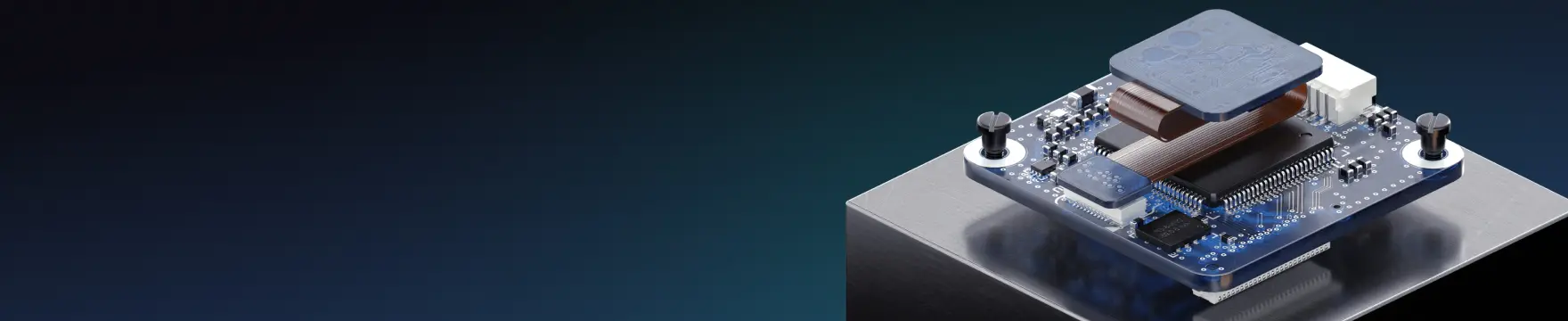
2020 was a year of firsts for most of us, and one big “first” for many people was remote working. Now, every company has their preferred set of collaboration and communication apps for working remotely or for management of complex projects. Then there are version control and revision tracking platforms like Github, which engineering teams need to enforce some level of order and organization in their projects. With technology development, the focus always gets put on software engineering, but what about hardware and electronics?
With the right collaboration tools and a bit of integration, you can create a cloud-connected design environment like Jira for hardware development projects and PCB project management. With a bit of light coding and a few worker applications, you can build your own managed environment that integrates with your design tools. If you’re not a software developer, but you still want to use proven management methodologies in your hardware projects, you can use platforms like Git or Jira for hardware development and project management.
What is Jira for Hardware Development?
Jira is part of a family of software products that teams can use for managing all types of work. Originally, Jira was used for bug tracking in software development projects, but it has evolved into a test/requirements management system and agile project management system. Technically, these functions within Jira could be used for any type of project involving issue tracking and management, including documentation, hardware, and software. Add to this the project management features, and you have an entire system for overseeing complex projects with multiple collaborators.
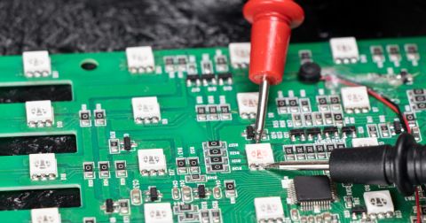
What PCB Designers Can Do With Jira
PCB designers and engineers that want to use Jira for hardware development can benefit from some of the following features:
- Track design defects on custom dashboards
- Leave comments in dashboards on defects and track history
- Control user access
- Customize views and workflows for your team
The dashboard-based interface in Jira resembles other project management tools and gives hardware designers some centralized control over their projects and teams. However, it doesn’t provide direct integration with PCB design software. This is where Git (or Github) has an advantage over Jira as it can be brought into your PCB design process and has closer integration with your design tools.
Using Jira vs. Github for Hardware Development
With all the focus recently on applying agile methodologies to just about everything, PCB designers and electronics engineers have started looking to platforms like Jira for hardware development and project management. Jira is great for project management, but it does not provide the same version control features as Github. I don’t know a single software developer that isn’t familiar with Github, but this is not always the case with hardware developers and PCB designers.
Based on the original Git version control system implemented for the development of Linux, Github provides a convenient way to store code repositories, track revisions to projects, rollback to previous project versions, and clone projects. Compared to Jira, Github is more focused on storing and sharing project data, not on project management.
Both Jira and Github can be used for hardware development generally; they aren’t confined to software development, even though that was their original use case. At their core, both platforms are designed to facilitate collaboration, even though their intended use cases are not the same. The table below provides a deeper comparison of these two platforms and how each of these platforms fit into a collaborative hardware development team.
If you’re an electronics engineer with a history of software development experience, then you’ll be comfortable setting up your own Git-based environment for managing your PCB design projects. Here are some great guides on creating a Git-based workflow for Altium users:
- How to "Git" Collaborative with Altium
- How to Create a CI/CD Pipeline for Your PCB Design
- Automated Mirroring Between Concord Pro and Your Git Server
- Git Tagging and Git for Hardware Development in Altium
Altium Agile Teams Gives PCB Designers the Best of Jira and Github
If you don’t have software development experience, Altium Agile Teams provides an easy-to-use collaboration and sharing system that gives you the best of Git and Jira for hardware development. Every Altium Agile Teams user can take advantage of the industry’s best PCB design collaboration platform. Altium Agile Teams helps unify your project management and revision tracking with these features:
- Full version control based on Git, including simplified revision tracking and project rollback features
- Instant sharing with other designers, customers, and manufacturers
- Full control over user access to your Altium Workspace
- Manage all projects, components, templates, and project releases in one place
- Commenting and comment history tracking features for all designs, including directly in a schematic or PCB layout
- Manufacturers can inspect and review all fabrication data before a design enters fabrication
Altium Agile Teams gives PCB designers a practical way to combine project tracking and revision control in a collaboration environment built specifically for hardware development. Learn how Altium Agile Teams helps distributed hardware teams coordinate design work, manage revisions, and collaborate securely →

About Author
Related Resources


Related Technical Documentation

Table of Contents
Speed at Scale. Structured Repeatability. Secure Flexibility.
- Start up fast with out‑of‑the‑box workflows
- Collaborate using ECAD‑MCAD codesign tools
- Manage BOMs with live supply chain part data
- Manage access and security as teams scale
Contact Us
Thank you, you are now subscribed to updates.