


Top 4 Time Wasters in PCB Design Collaboration

At a Glance
PCB design collaboration doesn’t have to be difficult when you use the right project management and communication tools.


Don’t let your time get wasted during PCB design collaboration. Try these strategies and tools instead.
An essential aspect of project management is time management, especially when your design team is working remotely. Your time management strategy is team-based and individual, but time can easily get spent on important tasks when working as part of a team. So how can you streamline important collaboration tasks for your design team to increase productivity?
The first step is realizing where time is being wasted during design, followed by finding the right tools to streamline communication, sharing, and collaboration on complex PCB designs. After managing a remote team of PCB designers, I’ve taken some pains to reduce time spent on tracking design progress, communicating with stakeholders, and getting designs completed on-time. If any of these resonate with you, there are some simple cloud collaboration tools that can save your design time.
Four Time Wasting PCB Design Collaboration Problems
Even if you’re a PCB design expert, working with customers and other team members in a remote environment requires communication and sharing tasks that can delay any project. Here are some of the top time-wasters I’ve noticed while working with team members.
Getting Questions Answered by Customers and Stakeholders
For me, this is probably the top time waster during a project. Design cycles are extremely short, and anytime a question arises for the customer it needs to get resolved quickly. Some design questions can stall an entire project, not to mention hold up moving to manufacturing. Even worse, some customers might want to take a hands-off approach; they assume you can read their mind, so they don’t make themselves available for questions.
Whenever there is a question on a design, or you need to flag an error for the customer, you can’t go further until you get their input. If questions go unanswered, the design gets held up and the schedule gets pushed back; no one is happy when this happens. Some common questions for customers and project stakeholders relate to:
- Errors in a design document. Our customers will sometimes provide schematics or a layout with some component placement. Errors aren’t always obvious when you start a complex PCB layout, and you might be partially through a layout before something serious is noticed. If there is a problem in either of these, the customer needs to resolve this quickly before a PCB layout can get finished.
- Unavailable or obsolete components. When ideal components are unavailable or obsolete, you need to notify the customer and provide suitable alternatives. It helps to have supply chain visibility tools to quickly find alternative components, ensure they’re in-stock, and get prices.
- Must-haves and nice-to-haves. Some design requirements cannot be violated (must-haves), such as mechanical requirements for an enclosure (this is one of the most common for me). Other requirements can be compromised (nice-to-haves), but there needs to be a protocol for implementing changes in case a design change might violate one of these requirements.
Implementing Design Changes as Specified by Customers
Once you do get clear responses from the customer or stakeholders, it can spawn another round of questions around reviewing and accepting the design changes. This back-and-forth process can involve screenshots of a design, email chains, and copious video chats. If you’re working on a regulated or sensitive product, such as an ITAR-regulated product, you need to use an FTP portal or other secure server to share design data. All of this takes up time, with most of the time spent waiting for responses to questions and reviewing design changes.
Communicating with Multiple Designers
Remote PCB design teams need a single set of tools for communication between team members. Slack and Skype are great for this, but quickly sharing and reviewing design data takes time as well; you might as well send around emails with screenshots and design files as attachments. Going back-and-forth between different communication channels, especially when reviewing and editing design data with team members, also takes up significant time.
My opinion on the matter is: try to consolidate everything into as few communication channels as possible. Ideally, you should have one chat channel per project, phone calls/text messages (emergencies only), and a tool for sharing and annotating design data (NOT email). Keep these channels dedicated for certain tasks and topics, don’t let people have a free-for-all in your chat channels. If you do use something like Skype or Slack for project communication, create a channel/room for each project to keep everyone on track.
Sharing Design Data
If you’re collaborating with a remote team, you need a tool to quickly share design data while tracking revisions in a single location and controlling user access. No one should have to deal with separate chains of design files, and team member visibility should be controlled when needed. The best cloud collaboration tools with integrate with your PCB design software while also providing revision tracking and user access control.
Once you’re ready to prepare for fabrication and assembly, these same sharing and communication tasks need to apply to your manufacturer. If you can (or if they’re willing), loop them into your chat channels with your lead designer. Sometimes, you’re at your manufacturer’s mercy as far as which communicating and sharing channels they prefer to use, but bringing your manufacturer into your design process early can help you get through a design review faster.

Solving PCB Design Collaboration Problems in the Cloud
From the list I’ve shown above, three of the four time wasting problems in PCB design collaboration revolve around communication. The communication aspect is understandable; people go on vacation or take personal time, they are involved in other projects that require attention, or they need to get an answer from a 3rd party. Tools like Slack, Skype, text messages, and old-fashioned email have their place, but real collaboration and sharing takes an integrated approach.
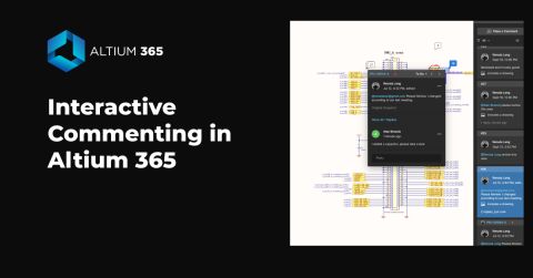
When you use Altium Designer on the Altium 365 platform, you’ll have access to supply chain data, commenting features, and data sharing tools to help you streamline PCB design collaboration. Your team can resolve questions and comments directly on design data rather than spending time using outdated communication tools for sharing data.
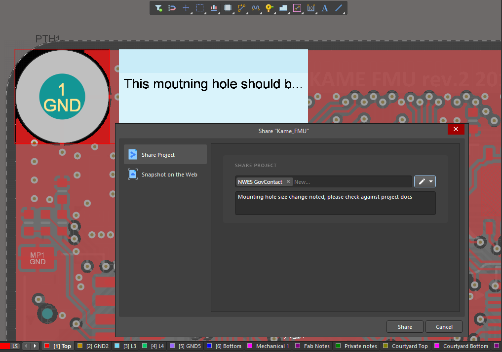
You’ll have access to many other features to help your team stay organized and work efficiently. Version control, user access management, and revision tracking features are built into the Altium 365™ platform. Your team can take advantage of a single tool for design data access, data sharing, and communication that integrates with Altium Designer.
Altium Designer® on Altium 365 is bringing an unprecedented amount of integration to the electronics industry until now relegated to the world of software development, allowing designers to work from home and reach unprecedented levels of efficiency.
We have only scratched the surface of what is possible to do with Altium Designer on Altium 365. You can check the product page for a more in-depth feature description or one of the On-Demand Webinars.

About Author
Related Resources
Related Technical Documentation
Table of Contents
Design to Release, Without the Friction
- Keep reviews tied to the right version
- Reduce handoff confusion and rework
- Spot sourcing and release risk earlier
- Work solo, share when needed
Get Started
Thank you, you are now subscribed to updates.