


Thermal Relief Design Guide

At a Glance
The CAD tools in Altium are ideal for thermal relief design for SMD pads and through-hole pins.


One of the most common PCB assembly defects discussed in guides on DFA is tombstoning, with the second most common probably being cold joints, with the latter being pointed out specifically on through-hole pins. While these two may not seem to be related, they are both related to heat flowing away from a pin or pad on a component. In PCB layout, this is addressed by adding a thermal relief pad onto the affected component so that heat is confined during soldering.
The question then becomes: when should you apply thermal pads, and which components will need them? Some DFA guidelines communicate the use of thermal pads as something that is needed everywhere, and sometimes the default design rule in a PCB or a project will enforce this across your design. In this guide, we'll break down how to select the right settings for your thermal pad and where to apply them.
Where to Apply Thermal Reliefs
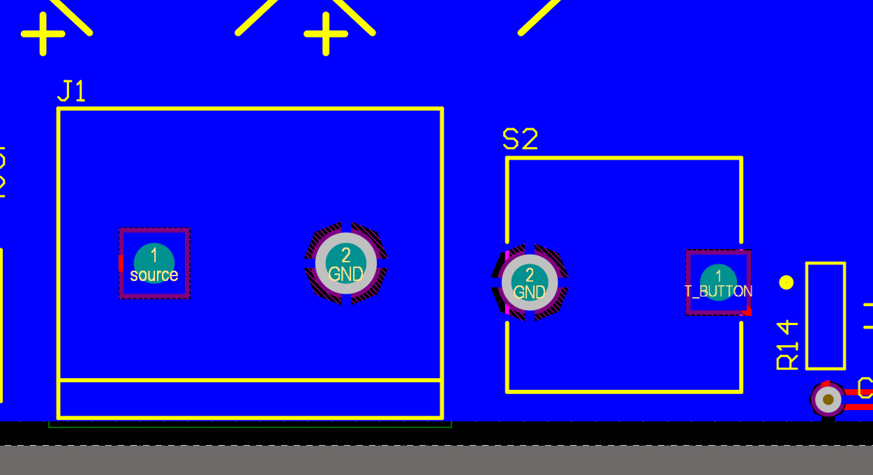
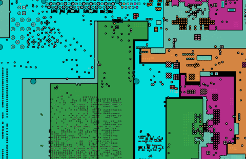
A simple image of thermal relief in a PCB layout is shown below. These thermal reliefs consist of small spokes connecting copper to a pad for an SMD component or through-hole pin. These thermal reliefs are applied automatically in your CAD tool, so you do not need to draw in the spoke connections, which have small traces or fill regions.
Thermal reliefs on through-hole pins.
Here we see two instances where it is recommended to apply thermal reliefs:
- On mask-defined SMD pads, i.e., pads on copper pour
- On through-hole pins where a pad makes a connection to a plane
Thermal reliefs are not necessary in the following instances
- On mask defined SMD pads connecting to a small copper pour
- On through-hole pin pads connected to a small copper pour
- On vias connecting to copper pours or planes, even if the pour connects to an SMD pad
The last point is quite important because it is technically possible to put a thermal relief onto a via. Frankly, there is no value in putting a thermal relief onto a via that connects to a pour which also connects to an SMD pad. If you need the thermal relief, just put it on the SMD pad instead of on the via. The goal is to confine heat to the SMD pad, not to allow it to spread around a large piece of copper.
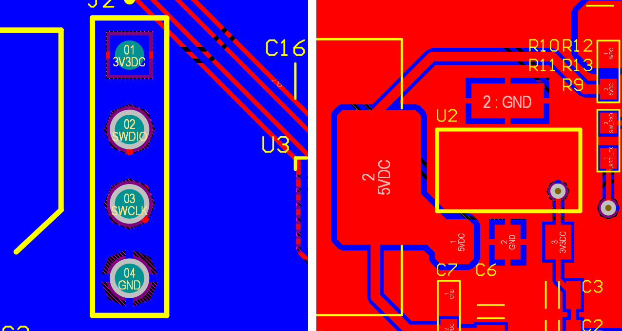
Left: thermal relief on through-hole pins for a pin header. Right: thermal reliefs on SMD pads connected to copper pour on the same layer.
There are a few other instances where thermal reliefs are not needed, especially on SMD components. These include:
- When a copper pour connection looks very similar to a trace
- On die-attached pads on integrated circuits
- When it can be guaranteed that heating is uniform across the board during soldering
The last point relates to the soldering process. In reflow, you are much less likely to require thermal relief pads everywhere. However, if you will be hand soldering all of your SMD components, particularly SMD passives, it may make sense to add thermal reliefs to the SMD pads for your passives. Hot air soldering or hot plate soldering is a bit of a wild card because it depends so heavily on the skill of the assembler and the equipment being used.
When is a Copper Pour Large?
This is an important question, as it will dictate when to place thermal reliefs on through-hole pins or on SMD pads. For through-hole components, we normally place the thermal relief on the connection to a plane. However, if we have a copper pour used on one layer instead of a plane layer, we essentially have the same thing: a large region of copper that can draw away heat from the pin and thus may need a thermal relief. The same effect occurs with an SMD component on a copper region, such as a large copper fill on one of the surface layers.
But if you connect one of these components to a polygon on some layer, does every single polygon need to have the thermal relief? I think the answer is "no."
- When the copper pour is very small, it looks similar to a trace and no thermal relief should be necessary.
- When an internal layer copper pour is very large, it looks a lot like a plane and a thermal relief would be necessary on through-holes.
- When a surface-layer copper pour is large enough to fill most of the surface, it also looks similar to a plane and a thermal relief would be necessary.
Somewhere in between very small and very large copper pours is a point at which a thermal relief on a component pin or pad starts to become necessary. It is quite difficult to predict what this is without running a test coupon for a large batch of boards through soldering. One would also expect a difference between reflow soldering and hand soldering. While this could be simulated, a better approach is to accept that the point where thermal reliefs become necessary has to be determined from quality inspections of assembled boards.
How Should Thermal Reliefs Be Designed?
Designers do not need to put a huge amount of effort into creating a thermal relief. Typically, a simple spoke connection from the four sides of a pin or pad will be acceptable. The size of the spokes on the traces and the clearance or opening size should be selected so that the edge features are not too small. Don't make the pad spoke so thin that you drop below your etch limit. Also, make the opening around the pad large enough that you stay above the edge clearance limit.
Typically, 8 mil traces with 10 mil clearance will be fine for the majority of components. For much smaller case passives that will be placed at high density, the trace width and clearance can be made smaller in order for the traces to fit around the pad.
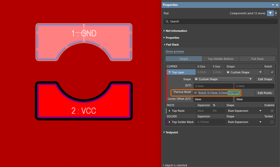
Thermal relief applied on a custom pad in Altium.
Thermal Relief Design in Altium
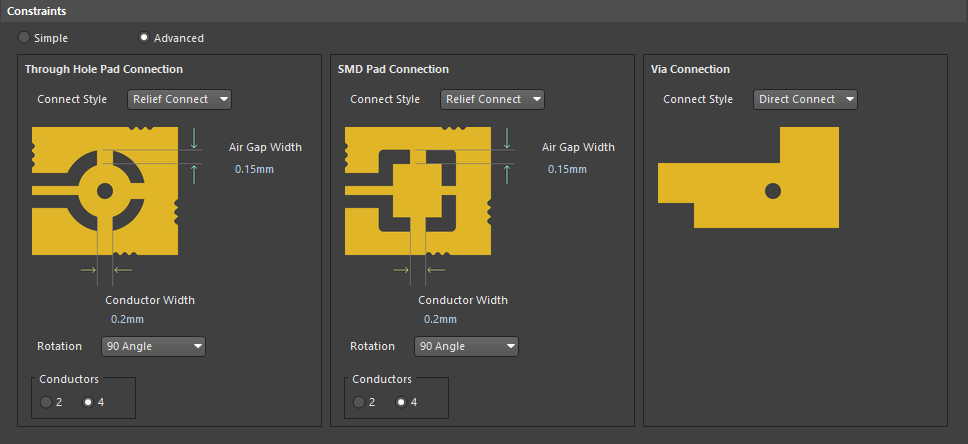
Altium offers multiple ways to implement thermal relief pads on SMD parts and through-hole components. These can be applied globally or selectively as follows:
- Applying a thermal relief style by using a plane or polygon connect design rule
- Applying thermal relief pads using design rule but with scope set to specific footprints or component classes
- Applying a thermal relief pad to a specific SMD pad or through-hole pin based in the pad/pin properties
The design rule system and query system in Altium allows you to mix and match these approaches for different types of components or groups of components. If you use the design rules, you will always have the option to manually apply thermal relief on specific through-hole pins or SMD pads.
To learn more about applying thermal relief pads in your PCB layout, check out these links in the Altium documentation:
Whether you need to build reliable power electronics or advanced digital systems, Altium Develop unites every discipline into one collaborative force. Free from silos. Free from limits. It’s where engineers, designers, and innovators work as one to co-create without constraints. Experience Altium Develop today!

About Author
Related Resources
Related Technical Documentation
Table of Contents
Design to Release, Without the Friction
- Keep reviews tied to the right version
- Reduce handoff confusion and rework
- Spot sourcing and release risk earlier
- Work solo, share when needed
Get Started
Thank you, you are now subscribed to updates.

