


Online PCB Design Review with Altium 365


You can design a PCB any way you like, but if it doesn’t pass a PCB design review and manufacturability checks, then it will never become a real board. A PCB design review is about more than just checking DRCs, it’s about designing to satisfy your manufacturer’s capabilities and processes. PCB design reviews also give the design team a chance to examine manufacturing files and deliverables for any errors before sending data in for fabrication and assembly. Manufacturers will normally conduct a basic PCB design review to qualify a board against their capabilities, but design teams should still take time to put their files through a thorough review before releasing a design to production. If your team can identify and correct errors before production, you can speed up your time to market and help ensure quality and yield once your design moves into high volume production.
Although many designs have become more advanced, the tools available for design review have lagged behind desktop design software. A cloud collaboration platform like Altium 365 allows you to instantly share design data with a manufacturer, other designers, or customers in a secure online interface. Designs can be viewed by any member of a team before a design is released for production, and manufacturers can quickly pinpoint specific points in a PCB layout that require changes to ensure yield and quality. Before you invest in third party software to support your PCB design review process, see how effective collaboration in Altium 365 can help you speed through a PCB design review.
What if you could get through the PCB design review process quickly, and all within your PCB design application? With the cloud collaboration tools in Altium 365, you can quickly place your data in a cloud repository and share it with other designers or a manufacturer. This platform is instantly accessible in Altium Designer, and it allows anyone on your team to pull data from the cloud back to their local machine for editing. This helps you quickly move through the PCB design review and qualification phase on the way to manufacturing.
What Goes into a PCB Design Review?
Once you’ve pushed your design data to your manufacturer, they will look over your layout, assembly, and Gerber files, and your BOM to make sure your board can be produced at scale. Your manufacturer may need to note some required changes to your design, or they may need to make the changes on their own. Both tasks can be completed quickly when your design data is accessible by designers and manufacturers directly within Altium Designer.
All these tasks are enabled in Altium 365, which also provides a direct pipeline into your manufacturer’s version of Altium Designer. Some important points that should be checked during a PCB design review include:
- Keep-in/keep-out areas
- Pad-to-trace, pad-to-pad, and pad-to-via clearances
- Drill bit/via sizes and minimum trace widths
- Silkscreen clearances
- Unconnected planes, pads, and vias
- Mismatch between Gerber data and your layout
If a manufacturer spots any of these in your design data, they can import your data into Altium Designer and make the changes on their own. Alternatively, a manufacturer can make notes in your design within an Altium 365 workspace. Some other important tasks that can be performed in Altium 365 and Altium Designer as part of a PCB design review are shown below.
Running ERCs and DRCs Online
ERCs and DRCs can be run directly within Altium 365. Any violations can be flagged within the online workspace, just as they normally would in Altium Designer. If you’re a manufacturer, you can scan through all layers in a design to spot any DRC errors or DFM violations. If you’re a designer, you can open your copy of Altium Designer and import the project from the Altium 365 workspace and make edits yourself. More complex changes can also be noted directly in the PCB layout as comments within the Altium 365 web instance or inside Altium Designer. This method of sharing the design through the cloud and allowing your collaborators to directly attach comments helps speed up the design process and helps greatly clarify the required changes to the schematics or PCB layout.

Running an online DRC in Altium 365
Annotating Schematic and Layout Data
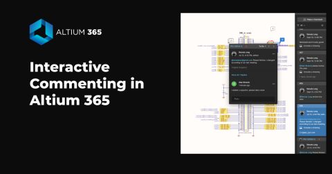
It’s common for multiple members of a design team, or the designer and the end customer, to collaborate and comment on a design as it’s being created. Within Altium 365, a designer or manufacturer can leave a comment directly on a component or respond to a comment from another user. Once you leave a comment, other team members will be able to see and resolve comments in the Altium 365 workspace. They can then import the design into Altium Designer and make any changes, then the design can be pushed back to the Altium 365 web instance.

Annotating a pad location in Altium 365
Adding or Moving Test Points, Mechanicals, and Components
Once annotations have been provided, you may need to move components, mechanicals, and/or test points in your design. Placing test points in a board is easy with the component creation features in Altium Designer. You can place test points as schematic symbols, and you can define a pad shape/size for your test point in your PCB layout. You can then store your new testpoint in your Altium 365 workspace for use in a new design. The same process you use to create, modify, and move test points can be used for proprietary components and mechanicals in your design.

Importing a component from Altium 365 into Altium Designer.
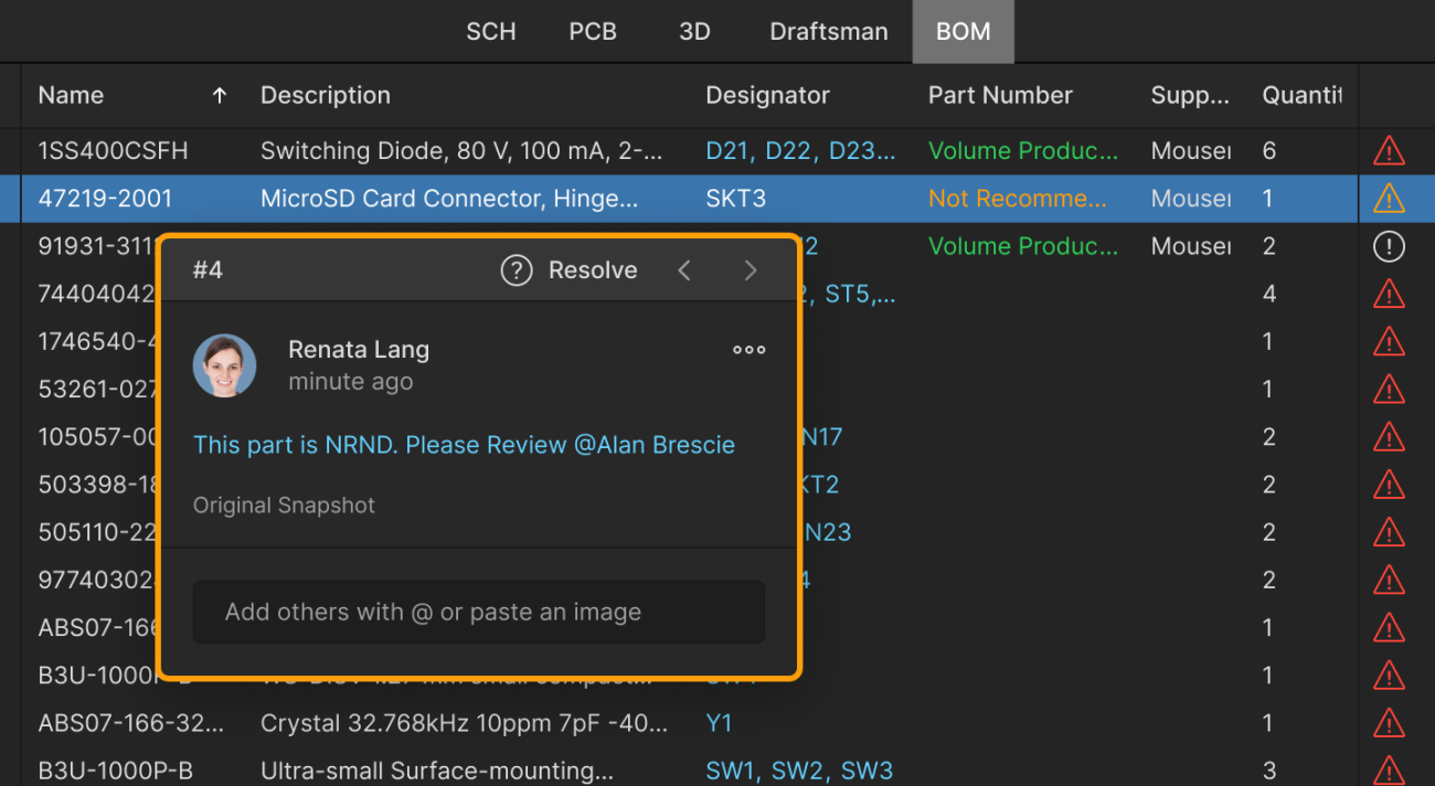
BOM Review
One of the important tasks in a project is to review the BOM for any parts that may be out-of-stock, NRND, obsolete, or EOL. While PCB designers should try to do this near the beginning of the PCB layout, the electronics supply chain moves quickly and it's possible for parts to become out-of-stock after they are reviewed and approved for use in a design. Platforms like the BOM Tool in Octopart are very useful on the front-end, but Altium 365 can leverage Octopart's data for an online PCB design review on the back-end before a design is sent out for quote.
Inside Altium 365, the BOM for a project can now be viewed and commented as needed in order to identify NRND/EOL/obsolete parts, out-of-stock parts, and incomplete part data. These features integrate with industry-leading supply chain data providers to give you the most accurate and up-to-date information on your parts without needing to browse distributor websites.
For a more advanced supply chain experience, Altium 365 offers a new feature for supply chain managers: the BOM Portal. This new feature enables teams to quickly scan through their design data, create purchases, and access supply chain data from a single dashboard.
Mechanical Backchecking in MCAD Software
Taking a systems-level approach to PCB design and manufacturing requires considering the enclosure and how the board will fit into a completed product. For over two decades, the mechanical backcheck process involved MCAD file exchanges, where the electrical designer would export a set of vendor neutral design files and send these to a mechanical design. Next, the MCAD user would have to import these into their software and manually regenerate the enclosure data around the PCB layout. If any interferences were spotted, these would have to be noted and manually communicated to the PCB designer so the layout could be changed and interferences could be eliminated. This process would normally require several iterations during a single PCB design review phase.
Mechanical constraints often impose limits on the PCB layout, and these would need to be defined as keepouts in a definite board shape before component placement. MCAD users need to be able to take a more active role in the design as well as have a method to streamline the backchecking process. Altium 365 and the MCAD CoDesigner plugin now allow an MCAD designer to more easily participate in the PCB design review process and help expedite design changes driven by mechanical backchecking. This all happens inside the ECAD and MCAD applications through a push-pull process instead of using manual IDX file exchanges.

A PCB designer can provide a 3D model of the PCB to a Solidworks user through Altium 365.
Compare Gerber Files Between Design Revisions
As designs are modified and deliverables are prepared for manufacturing, important changes are often identified in the manufacturing files before the design is finalized and released. The ability to compare Gerber files between revisions provides a convenient way to see specific changes that were implemented in the PCB layout after each review. Altium 365 includes a feature that allows each version of Gerbers produced during the design phase to be viewed and compared in collaboration with customers, a manufacturer, or another team member. This happens through the Altium 365 web interface, allowing anyone to participate in the design review process, even if they are not an Altium Designer user. Gerber differences are called out visually so that they are as easy as possible to identify, and the required changes can then be noted directly in the PCB layout or schematics using the Comments feature.

The Gerber compare utility in Altium 365 allows design differences between two sets of fabrication files to be seen visually.
Reduce PCB Design Review Time with Cloud Collaboration
The old way of sending files between team members via email is outdated, inefficient, and lacks security. The new way to share and collaboratively update your advanced designs is to use a cloud collaboration tool that integrates with your PCB design platform. Instead of using a 3rd party data sharing application or resorting to the old ways of sharing data, your cloud sharing tools should be accessible within your design software. Altium 365 is the only platform that provides the important collaboration tools modern design teams need and makes them accessible inside Altium Designer. From popular MCAD applications to a complete file sharing system with integrated version control, Altium 365 gives enterprise design teams the tools needed to move their designs into full-scale manufacturing.
In addition to collaborative design with your team members, a designer can also invite a manufacturer into an Altium 365 workspace so they can participate in a design review and note required changes in a design. A manufacturer can also be given easy access to project releases to help expedite the PCB design review process, help you source and manage components, and quickly take a design into production. Manufacturers that are invited into a workspace will be able to quickly identify and pinpoint any required design changes using the tools provided above, or designs can be downloaded into 3rd party applications for further review. No other platform gives design teams a complete set of tools needed to manage design data and collaborate in a secure cloud-based platform.
- Your CAD tools and layout features will be accessible alongside important collaboration tools and management utilities when you use Altium Designer.
Learn more about working in Altium Designer’s integrated environment.
- Adding Altium 365 to Altium Designer lets you push any designs to a cloud workspace. This provides instant collaboration and control over your design data in a secure environment.
Learn more about integrating Altium 365 and Altium Designer.
- When you use Altium Designer and Altium 365, you’ll have access to the only data management platform that integrates your component, supplier, and design information into a complete management solution.

Take control over all aspects of your PCB design review process with Altium Designer and Altium 365.
Altium 365 provides these important design collaboration features and much more directly within Altium Designer. When you use Altium Designer, you’ll also have access to the industry’s best layout and routing features in a rules-driven design environment. You’ll also be able to instantly create your manufacturing documentation and send it to your board house for fabrication.
Fusing Altium Design and Altium 365 gives you the only platform that makes your important design documentation accessible from anywhere. If you’re ready to speed through your next PCB design review and streamline your data management processes, it’s time to try Altium 365.

About Author
Related Resources
Related Technical Documentation
Table of Contents
- What Goes into a PCB Design Review?
- Running ERCs and DRCs Online
- Annotating Schematic and Layout Data
- Adding or Moving Test Points, Mechanicals, and Components
- Mechanical Backchecking in MCAD Software
- Compare Gerber Files Between Design Revisions
- Reduce PCB Design Review Time with Cloud Collaboration
Design to Release, Without the Friction
- Keep reviews tied to the right version
- Reduce handoff confusion and rework
- Spot sourcing and release risk earlier
- Work solo, share when needed
Get Started
Thank you, you are now subscribed to updates.


