


When Does Decoupling Capacitor Location Matter on a PCB?


Decoupling capacitor placement is one of those PCB layout topics where a simple rule gets repeated far beyond the conditions where it is actually useful. The standard instruction is familiar: place the capacitor as close as possible to the power pin. Designers hear that from datasheets, application notes, layout checklists, and AI-generated diagrams that show capacitors packed around every IC like a decorative border. The problem is that this advice compresses several different PDN structures into one rule, and those structures do not behave the same way.
Once the inductive path between the capacitor and the load is defined, the placement decision becomes much easier. In some boards, moving a capacitor even modestly farther away raises path inductance enough to make the part less effective. In other boards, especially multilayer designs with closely spaced power and ground planes, the exact capacitor location can become much less sensitive because the planes provide the low-inductance current path.
Background on Decoupling Capacitor Placement
Some of the mythbusting activity surrounding decoupling capacitor placement traces back to Dr. Todd Hubing’s IEEE paper on multilayer PCBs with internal power and ground planes. That paper examined whether familiar placement rules from one-sided and two-sided boards still applied once a board used a low-inductance plane pair. The key result is the one that still drives debate today: when decoupling capacitors are connected into closely spaced planes (<10 mil), the measured power bus impedance can show very little sensitivity to capacitor placement location, provided the capacitor is not placed excessively far from the load.
That result is useful, but it is also easy to overgeneralize. Hubing’s conclusion was not that capacitor location never matters. The point was that closely spaced plane pairs change the dominant inductance in the current path, which changes how strongly capacitor location affects PDN impedance. That is a very different statement from saying every board can ignore capacitor placement.
Read Dr. Hubing’s paper here:

Graph from Hubing et al. showing overlapping impedance curves for capacitors placed at multiple locations on a multilayer board with closely-spaced power and ground planes.
Component Package Determines Whether Placement Matters
The statement that capacitor location “does not matter” is an overgeneralization; capacitor location matters differently depending on the package, PCB stackup, and how the capacitor is tied into the PDN.
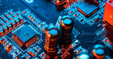
Consider a leaded package compared to a BGA. With a quad flat pack or similar part, the power pins are exposed at the package perimeter, and a nearby capacitor can often be tied directly to those pins with short traces. In that configuration, the route between the capacitor and the load becomes part of the power path impedance.

QFN/QFP or similar packages have leads exposed around the edge of the component, which allows a direct connection with traces. Note the connection on the GVDD net,where the trace connection is used and has high path inductance per unit length.
That arrangement minimizes path inductance because the current loop remains compact and the trace contribution stays small. In these packages, the usual placement advice makes practical sense because the pin arrangement was built to support that connection style. Note that you could use a power plane with these packages, but the plane is generally not required only for leaded packages.
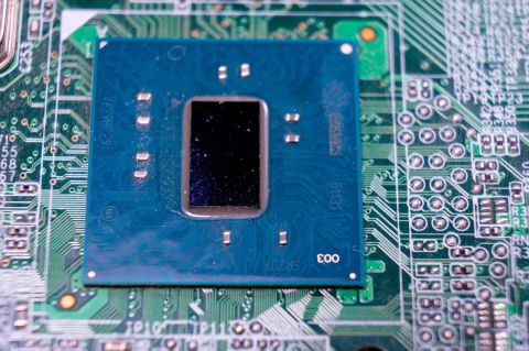
Large BGAs typically have multiple interior power and ground balls clustered in the interior region of the package. No one is going to route individual traces from capacitors sitting outside the package into the center of the part. Unless you put the capacitors on the back side of the BGA, you are going to rely on power and ground planes and vias into those planes.

In large BGAs, the interior of the BGA will many of the PWR and GND pins clustered near the center. Pink pins = PWR, blue pins = GND. Example above is for an i.MX processor.
For large BGAs, that same direct attachment method with traces is impossible because the power and ground pins are numerous and buried under the package body. So in this package, you need to have plane connections in internal layers in order to reach the pins near the center of the package. The question is then whether to use close power-ground plane spacing as this will affect the path inductance.
Path Inductance
To determine whether the placement location matters, we need to know the total inductance along the path. That total path inductance is the capacitor’s own ESL, the mounting inductance of the pads and vias plus the routing inductance between the capacitor and the device pins.
We can write the path inductance as:
L(path) = ESL + L(mount) + L(trace or plane)
A useful order-of-magnitude estimate for trace inductance is about 5 to 7 nH/inch, with about 7.5 nH/inch for a 50 ohm trace on a typical Dk = 4 laminate system. Those are large enough values that even modest routing length becomes relevant. If the capacitor already contributes around 3 to 3.5 nH of mounting inductance, then adding appreciable trace length can quickly double or triple the total inductance seen between the capacitor and the load.
What about planes? A plane pair has spreading inductance, which is commonly expressed in inductance “per square.” That is a useful way to think about the plane pair because the total inductance depends on the length-to-width ratio of the current spreading region and the spacing between the planes. For closely spaced planes, typical values can be on the order of 100 pH/square.

Current path between a decoupling capacitor and an IC in a BGA package. The inductance along this path is known as spreading inductance.
Some plane spreading inductance and plane capacitance (typical FR4 Dk) values are given by AMD in the table below. Note that the value of 130 pH/square for a 4 mil plane separation is very close to the rule-of-thumb value given by Bogatin (32 pH/square/mil, or 128 pH/square on a 4 mil thick dielectric).
Dielectric Thickness | Inductance | Capacitance | ||
| (micron) | (mil) | (pH/square) | (pF/in2 ) | (pF/cm2 ) |
| 102 | 4 | 130 | 225 | 35 |
| 51 | 2 | 65 | 450 | 70 |
| 25 | 1 | 32 | 900 | 140 |
Spreading inductance aside for a moment, you need to use planes in general in large BGAs because it is the most efficient way to access the large number of power and ground pins in the interior of the package. At minimum, you need large copper pours that look a lot like planes. Both options provide much lower inductance than a trace connection, as we’ll see below.
Example: Plane Connection vs. Trace Connection
This gives us two situations to compare: trace routing into the PWR/GND pins on a leaded part vs. plane routing into a BGA. Once the capacitor is tied into a closely spaced power and ground plane pair, the placement problem changes because the planes carry the current between the capacitor and the component. In that case, the dominant distributed inductance is no longer a long routed trace, it is the spreading inductance in the plane pair.
At that scale, even a fairly large board region can contribute less inductance than a much shorter trace route. A simple comparison makes the point clearly. Suppose a capacitor is located 5 inches from the load:
- If that connection is made with a wide trace at only 5 nH/inch, the routing inductance alone is 25 nH
- Adding approximately 3 nH of mounting inductance gives a total of about 28 nH
Now take the same 5 inch separation and assume the current travels through a 5 inch by 2 inch power-ground plane region, which is 2.5 squares:
- At 100 pH/square, the spreading inductance is about 250 pH, or 0.25 nH
- Add the same 3 nH of mounting inductance and the total is about 3.25 nH
The physical distance is identical in both cases, but the connection method changes the total inductance by nearly an order of magnitude.
This is the context behind the not-so-familiar result from Hubing’s work. If a capacitor has about 3 nH of mounting inductance and the plane path only adds a fraction of a nanohenry, then moving the capacitor around on the board may not significantly change the total path inductance. Under those conditions, the capacitor’s exact location is less sensitive than many application notes or guidelines would imply.
Placement Guidance Depends on the Connection Method
In summary, the best location for a decoupling capacitor is one that minimizes inductance (path + mounting). The mounting inductance (ESL + pads/vias) is invariant with location, while the path inductance may depend heavily on location. From the above discussion of trace inductance vs. spreading inductance, it should be clear that the trace length raises inductance to a much greater extent than routing with planes or large rails.
In multilayer boards with tightly coupled power and ground planes, low spreading inductance can make capacitor location much less sensitive, especially under BGAs where plane access is the natural implementation. For QFNs, QFPs, and similar leaded packages, the designer can often connect the capacitor directly between nearby VDD and VSS pins with short traces.
Whether you need to build reliable power electronics or advanced digital systems, use Altium’s complete set of PCB design features and world-class CAD tools. Altium provides the world’s premier electronic product development platform, complete with the industry’s best PCB design tools and cross-disciplinary collaboration features for advanced design teams. Contact an expert at Altium today!
Frequently Asked Questions
Does decoupling capacitor placement always need to be as close as possible to the power pin?
No, but this depends on the component package. That rule is useful in some layouts, but it does not apply equally to every PDN structure. This depends on the inductive path between the capacitor and the load.
Why do BGAs usually require plane connections for decoupling capacitors?
This is because the power and ground pins are buried under the package, often near the center of the package. Direct trace connections from nearby capacitors to these pins are not possible, so planes and vias become the normal connection method. The other method is to place decoupling capacitors on the back side of the BGA region and connect to the pins with via-in-pad.
What is path inductance in a decoupling capacitor connection?
Path inductance is the total inductance between the capacitor and the load. In the article, it is defined as the capacitor ESL plus mounting inductance plus the routing inductance from traces or planes.
How do closely spaced planes affect PDN impedance?
Closely spaced power-ground planes reduce spreading inductance, so capacitor location can become much less sensitive. Closely-spaced power and ground planes also form an effective low-inductance capacitor which can supply power to large ICs at high frequencies.

About Author
Related Resources
Related Technical Documentation
Table of Contents
Design to Release, Without the Friction
- Keep reviews tied to the right version
- Reduce handoff confusion and rework
- Spot sourcing and release risk earlier
- Work solo, share when needed
Get Started
Thank you, you are now subscribed to updates.

