


What is Spreading Inductance?

At a Glance
The spreading inductance of a plane pair has a simple meaning, but it can be difficult to calculate. Here are some points designers should know about the spreading inductance of a plane pair.


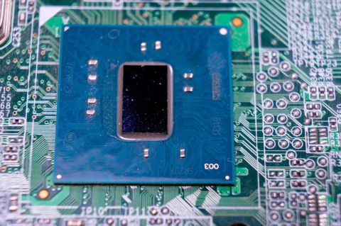
The above image shows a PCB with two large capacitors that might be used as the output caps for a VRM, which then can supply DC power to an integrated circuit. However, this board hides an important source of inductance: the power plane and power rails.
If you’re working with a high speed digital component, there are some simple power integrity rules that should be followed. Using plane pairs, decoupling capacitors, and bypass capacitors are the starting point for designing the PDN in your PCB to have the required impedance. There is one quantity that is sometimes ignored when building a PDN impedance simulation: the spreading inductance of your plane pair. This quantity plays a deceptively simple role in determining the inductance leading into the input power pin on a component.
What is Spreading Inductance?
All conductive elements in your PCB can have some parasitic elements, including plane pairs. The one that we normally care about is plane capacitance, which provides additional capacitance to help your PDN decouple at high frequencies. In a DC PDN simulation, we look at the DC conductivity to try and spot power loss. There is one additional parasitic in a plane pair: the spreading inductance.
Simply put, the spreading inductance is the inductance created by the current path drawn along two planes and the circuit elements that connect them. In the PDN of a PCB, the spreading inductance is defined by the current loop spanning from a decoupling capacitor network, along a power plane, into the load input, and back along the ground plane to the capacitor. It is not equivalent to the loop inductance formed by this current path, it is only the portion of total inductance contributed specifically by the plane. The various contributors to plane-pair impedance are shown below:

Why should we use the term “spreading inductance”? The term is used to denote that the current “spreads” in the power and ground plane pair, it does not follow a straight line. The current is confined to a narrow region between the decap output and the via input. Rather than following a literal straight line between these two points in the plane, current spreads out in the plane but does not totally fill copper in the plane pair.
This confinement of the current in the plane has an important consequence for PDN design: eventually, increasing the plane area does not necessarily decrease the spreading inductance. This is because, with a large plane, the current will not continue spreading along the current path. Instead, you can only change two other distances if you want to modify the spreading inductance as follows:
- Reduce d: Bringing caps closer to the load IC reduces the spreading inductance
- Reduce h: Bringing the plane layers closer together reduces the spreading inductance
However, reducing both values by the same proportionality constant has no effect on spreading inductance! This is because spreading inductance is a "per square" measurement, as I discuss in the next section.
How Large is Spreading Inductance For a Plane Pair?
Unfortunately, there is no closed form equation you can use to calculate spreading inductance. The calculation involves several integrals with an eigenfunction expansion. The fastest way is to export your design into a field solver application. If you want to learn more, there is one comprehensive resource found in the research literature:
Spreading inductance is expressed as a "per square" value, where a square is the unitless ratio of the current path length to its width in the plane pair. Typical values for a closely spaced plane pair (3 to 5 mil dielectric separation) fall in the range of tens to hundreds of picohenrys per square. AMD, for example, publishes typical spreading inductance values on the order of 0.15 nH per square for a tightly coupled plane pair, and this value scales upward with increasing dielectric thickness between the power and ground planes. The table below shows AMD's data for spreading inductance and interplane capacitance for a power/ground plane pair from UltraScale Architecture PCB Design User Guide (UG583).
| Dielectric Thickness | Inductance | Capacitance | ||
|---|---|---|---|---|
| (micron) | (mil) | (pH/square) | (pF/in2 ) | (pF/cm2 ) |
| 102 | 4 | 130 | 225 | 35 |
| 51 | 2 | 65 | 450 | 70 |
| 25 | 1 | 32 | 900 | 140 |
Even at these low per-square values, the total spreading inductance accumulated over several squares between a decoupling capacitor via and the IC power via can reach the low single-digit nanohenry range. For example, suppose we have a 5 in. x 2 in. rail connecting a capacitor to the pins on a BGA package. The "square" in this case is the ratio of the length of the connection (5 in.) to the width of the rail making the connection (2 in.). If we have a 2 mil thick dielectric separating the plane pair, then the total spreading inductance would be:
L(2 mil) = 65 pH/sq. * (5/2) = 162.5 pH
This is enough inductance to limit the plane pair's ability to deliver stable, low-impedance power in roughly the 100 MHz to 1 GHz frequency range. Below 100 MHz, bulk and ceramic decoupling capacitors dominate the PDN impedance. Above approximately 1 GHz, the plane pair's spreading inductance becomes too large relative to the low impedance required by the load, and the IC's in-package decoupling capacitance and on-die capacitance take over as the primary charge reservoirs. The plane pair, therefore, occupies a specific middle band in the PDN impedance curve, and its contribution is bounded on both sides by inductance that it cannot overcome through geometry changes alone.
One consequence of this is that increasing plane area beyond a certain point yields diminishing returns. Because current does not spread uniformly across an arbitrarily large plane, the spreading inductance converges to a finite value even as copper area grows. The practical levers for reducing spreading inductance are reducing the dielectric thickness between the power and ground planes and reducing the distance between the decoupling capacitor vias and the load IC power vias.
Modeling Planes With Spreading Inductance
In general, linear time-invariant (LTI) electrical systems can be modeled as RLC circuits, and the same idea applies to a plane pair with spreading inductance. The image below shows how the spreading inductance along a power plane would be modeled in a schematic for use in a simulation. The portion of the plane connecting from C-Plane to OUT contains two elements: an inductance (L-Plane) and a resistance (R-Plane). L-Plane is our spreading inductance defined by the current loop formed in the PDN. Together with C-Plane, these three elements contain all parasitics related to a plane pair.

Technically, we would have additional elements along the GND net corresponding to the R-Plane value for the ground plane and an additional L-Plane element for the via connection, but we can lump this into the R-Plane/L-Plane elements if we like. What’s important is how connections would be made to other components in the above schematics. PWR is the output from the decoupling capacitor network. The series RL elements spanning from PWR to OUT model the location of the decoupling capacitor network.
Decoupling Capacitors Connected to a Plane
What about decoupling capacitors that are connected to a plane pair? Does the spacing between the capacitors have some inductance? The answer is "yes" it does, but this inductance is easily reduced by placing the caps very close together. We should be able to see this above: placing the capacitors close to each other basically sets d = 0.
As it turns out, the connection of decoupling capacitors connected directly to a plane pair is what allows more flexibility in the placement of the capacitors compared to connections with traces. This is an important distinction, and I think the high-speed PCB design rule regarding "place decoupling capacitors as close as possible to power/ground pins" originated from the usage of traces to connect decoupling capacitors to quad-pack ICs, not for connections to BGAs with power/ground planes.
Plane Connection vs. Trace Connection to a BGA
Consider a decoupling capacitor placed 1 inch away from the power via of a large BGA. We will compare two connection methods: a routed trace pair versus a closely spaced power/ground plane pair with approximately 4 mil dielectric separation.
For the trace connection, a typical microstrip or stripline trace contributes roughly 7.5 nH per inch of loop inductance. Over a 1-inch path, the trace adds 7.5 nH of path inductance. Combined with the capacitor's own 3 nH of mounting plus ESL inductance, the total path inductance is approximately:
L (trace) = 3 nH + 7.5 nH = 10.5 nH
For the plane connection using a tightly coupled plane pair at 0.15 nH per square, we need to estimate the number of squares in the current path. With a 1-inch separation between the capacitor via and the BGA power via, and current spreading to an effective width of roughly 1 inch in the plane, the path is approximately 1 square. The plane path inductance is then approximately 0.15 nH. The total becomes:
L (plane) = 3 nH + 0.15 nH ≈ 3.15 nH
The major contributors in these calculations are summarized below.
|
Parameter |
Trace Connection |
Plane Connection (4 mil spacing) |
|---|---|---|
|
Path inductance (1 inch) |
7.5 nH |
~0.15 nH |
|
Capacitor mounting + ESL |
3 nH |
3 nH |
|
Total inductance |
10.5 nH |
~3.15 nH |
The plane connection contributes less than 5% of the total path inductance, while the trace connection more than triples it. This result holds specifically for a closely spaced plane pair with approximately 4 mil dielectric thickness. A much thicker plane separation, such as 20 to 40 mils, would increase the per-square spreading inductance proportionally, and the plane path inductance would begin to approach values similar to trace connections, eroding the advantage.
This comparison reveals a practical point: when the capacitor is connected through a tightly coupled plane pair, the mounting inductance of the capacitor itself dominates the total. Moving the capacitor from 1 inch away to 0.5 inches away only saves a fraction of a nanohenry in plane path inductance, a change that is nearly invisible against the 3 nH mounting contribution. The placement flexibility that planes provide is real and quantifiable.
In this example, we see another reason power plane pairs are so important in BGAs:
- In BGA packages, the power pins tend to be clustered closer to the center of the package and there may be a large number of them. This requires a plane to make a connection between capacitors and the package.
- If a given capacitor has about 3 nH of mounting inductance and the plane path only adds less than 1 nH, then moving the capacitor may not significantly change the total path inductance.
- A good guideline to help further reduce the total inductance (mounting + path) is to use the smallest case caps that can still hit your required capacitance specs. 0402 case size is a good general-purpose selection for high speed boards unless you're designing to very high density and need 0201/01005 cases. In these caps, the ESR value will be non-negligible, which can actually be a good thing, and the ESL values tend to be lower.
A good guideline to follow is to use the smallest case caps that can still hit your required capacitance specs. 0402 case size is a good general-purpose selection for high speed boards unless you’re designing to very high density and need 0201/01005 cases. In these caps, the ESR value will be non-negligible, which can actually be a good thing, and the ESL values tend to be lower.
Via Connections on the Back Side of a BGA
The above discussion should illustrate why we prefer to use planes and take advantage of spreading inductance: it eliminates the inductance from a trace connection in the total path inductance. What if, instead of using a plane connection routed around the edge of a large BGA, we placed capacitors on the back side of the BGA?
Bringing decoupling capacitors to the back side of a BGA and connecting directly to the power/ground pins with via-in-pad effectively reduces the spreading inductance to near zero. In this case, the only inductance between the capacitors and the pins is the mounting inductance, which in this case comes from the capacitor ESL and the through-hole via connections to the BGA pins.

In this case, you might still have similar or larger path inductance as the case where you use the plane's spreading inductance. If the plane connection case uses blind vias, then the through-hole connection illustrated above will definitely have larger mounting inductance for those capacitors. Therefore, it is not always the case that placement directly on the back side of the BGA gives the minimum path inductance.
To summarize, extraction of inductance values along these various paths is difficult, but a good rule of thumb is to take advantage of the plane connections wherever possible to ensure low plane pair inductance up to high frequencies. Beyond 1 GHz, the package and die capacitances take over. Modeling this in EDA software is possible, including in a SPICE package, as long as the capacitances and inductances are known for each portion of the PDN model.
Altium Designer, included in Altium Develop, provides built-in SPICE package that supports a range of simulations, including PDN simulations. As designs move toward review and release, Altium Develop makes it easier to share the current design state when input from others is needed, without forcing changes to the way engineers already work.

About Author
Related Resources
Related Technical Documentation
Table of Contents
Design to Release, Without the Friction
- Keep reviews tied to the right version
- Reduce handoff confusion and rework
- Spot sourcing and release risk earlier
- Work solo, share when needed
Get Started
Thank you, you are now subscribed to updates.

