Delay Tuning for High Speed Signals: What You Need to Know
Length matched lines in a PCB
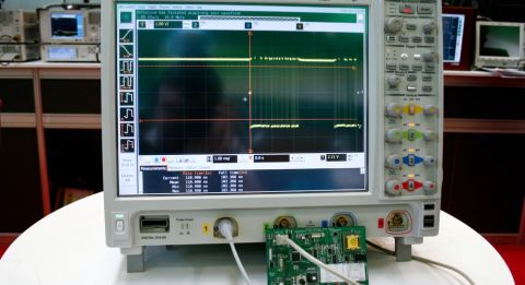
Take a look at two signal readouts on an oscilloscope, and you can see how length/timing mismatches between signal traces can improperly trigger downstream gates. The situation becomes worse when we look at the travel time for a master clock signal and the roundtrip time for sent/received data in different computer interfaces. SDRAM has solved this nicely by placing a clock in the slave device and sending a clock signal along with the retrieved data, while other interfaces (USB 3.0, SATA, etc.) extract the clock signal directly from the data.
For the rest of us, delay tuning among multiple parallel interconnects, traces in a differential pair, and with a clock signal ensures data arrives in the right place at the right time. Applying any length tuning scheme requires working with signal delay times in different signalling/interface standards, not just a simple length. Here’s what you need to know about designing for delay tuning and keeping signals synchronized.
Delay Tuning vs. Length Tuning
Length tuning and delay tuning basically refer to the same idea; the goal is to set the lengths of signal traces in a matched group of nets to the same length value. The idea is to ensure that all signals arrive within some constrained timing mismatch. When two signal traces are mismatched within a matched group, the usual way to synchronize signals is to add delay to the shorter signal trace by adding some meandering. Trombone, sawtooth, and accordion meandering are typical ways to add delay to a trace.
Whether you’re applying delay tuning between a clock signal and multiple signal lines, within a differential pair, or between multiple differential pair in the absence of a clock line, you need to know the specific timing tolerances for your signals. With differential pair receivers and components in SerDes channels, the limiting factors that determine the allowed length mismatch between each signal are the signal rise time and propagation delay in an interconnect.
Different interfaces that run at different data rates and with different signalling standards will specify different permissible length or timing mismatches. These mismatch values typically assume you are working on FR4, but more specialized designs on substrates with a different dielectric constant will carry different length matching constraints. When planning I/O channels in your board, you should look up these allowed length mismatch values for your board and convert this allowed mismatch to a timing mismatch (see the equation below).
Working With Timing Mismatch
Working with a timing mismatch instead of a length mismatch is the central idea in delay tuning. If you are working with PCB design software that only considers a length mismatch, then you need to calculate the correct length mismatch for your particular substrate. The length mismatch is equal to the timing mismatch multiplied by the signal velocity (units of in./ps) in your particular substrate:
Signal velocity equation (units: in./ps)
In general, a substrate with a larger dielectric constant causes the signal velocity to be lower, which increases the allowed length mismatch between two signals. Similarly, if you are overdriving standard components, you will have a shorter rise time (higher slew rate), which also places tighter constraints on your timing. To a first order approximation, if you halve the signal’s rise time, then the allowed timing constraint should also be cut in half.
The allowed mismatch is normally defined in terms of a tolerance on the clock period rather than the rise time. For a given clock period, the allowed length mismatch is inversely proportional to the signal velocity. With length mismatches being quoted with an assumed dielectric constant (e.g., FR4), you’ll need to convert the length mismatch using the signal velocity for your particular substrate material.
Phase Mismatch in Differential Pairs
The term “phase mismatch” is sometimes thrown around in the same breath as length tuning and delay tuning, but it has an important consequence when working with differential pairs. In some cases with differential pair routing, such as when a different pair needs to route through oddly-placed vias, there may be a short region where each end of the pair is uncoupled. This may arise in addition to the overall length of the pair being mismatched, and multiple pairs in a matched group may require length matching as well.
Phase matching requires adding some small amounts of copper at the mismatched end such that the lengths of the traces in the uncoupled region are length matched. This rather important for ensuring a differential pair can properly suppress common mode noise; any common mode noise induced in the uncoupled portion should propagate over the same distance to ensure it remains matched in both pairs once it reaches the receiver.
You won’t need to manually measure trace lengths when you define the right length tolerances as design rules.
Intra-Pair vs. Inter-Pair
Normally, when referring to delay tuning or length matching, we're referring to the two traces within a pair that is used to make a serial connection. However, you might need to apply delay tuning/length matching between two differential pairs. An example comes from DDR, where the differential strobe (DQS) and differential clock lines need to have length matching enforced. As an example, for DDR3, the allowed skew between these differential pairs is 5 ps according to Intel's guidelines.
Once the phase is matched in the uncoupled region, you should check that the remainder of the differential pair is appropriately length matched so that edge transitions fall within allowable skew limits. However, the length should be consistent throughout the pair if it was originally routed properly. When adding a length matching section to a differential pair as part when inter-pair skew compensation is needed, the length matching section should be placed symmetrically throughout the differential pair. Note that inter-pair skew constraints are typically looser than intra-pair skew values in order to provide sufficient common mode noise suppression and signal extraction.
More on Delay Tuning: Pin-Package Effect
Once the signal reaches a pin/pad on a particular component, it still needs to travel through the exposed conductor, along the bond wire into the interior of the package, and into the package die. The exposed conductor, pad/pin and the input to the internal circuitry has some parasitic inductance and capacitance, and the signal travels at a different speed as it traverses the bond wire compared to traveling on a signal trace. The bond wires also have some slightly different geometries, which adds different levels of delay to signals on different pins.
All device manufacturers should be able to tell you the pin-package delay, for a particular component. This is specified either as a delay in picoseconds, or as a length (usually mm or microns). You should be able to retrieve this delay value from the IBIS 6 documentation for the particular component. This length should be included when performing any type of delay/length tuning with signals in a differential pair or for multiple synchronized differential/single-ended signals.
With the powerful interactive routing and post-layout analysis tools in Altium Designer®, you’ll have a complete package built on top of a unified rules-driven design engine, allowing you to implement delay tuning for high-speed signals and important signal integrity simulations. You’ll also have a complete set of tools for building schematics, managing components, and preparing deliverables for your manufacturer.
Now you can download a free trial of Altium Designer and learn more about the industry’s best layout, simulation, and production planning tools. Talk to an Altium expert today to learn more.


