
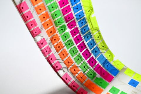


Unique Flex Termination Methods


I think it is important to know that basically any connector you would select for rigid printed circuit boards can also be assembled to a flexible circuit. Traditional thru-hole and SMT connectors, high density circular connectors, D-subminiature connectors, pin and socket connectors, leaded and unleaded, are all options to consider with flexible materials.
That said, I am going to veer slightly off topic with the caution to NOT forget to review and implement the recommended design rules when stiffeners are needed to help support the connector area. In many cases, the connectors themselves are heavier than the flex materials, which can cause stress and conductor cracking without an added stiffener for support. But, back on topic, in today’s blog, we will talk about a few termination methods that are more unique to flexible circuits; ZIF connectors, unsupported flex fingers and crimped contacts.
ZIF (Zero Insertion Force) Connectors:
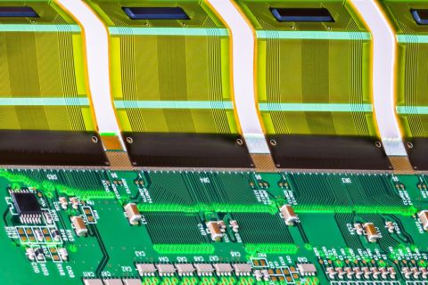
Zero Insertion Force connectors are one of the more increasingly popular connection methods with several benefits. The flexible circuit can be inserted and removed multiple times with little mechanical wear on copper traces. ZIF connectors often contain mechanical latching mechanisms that clamp down onto exposed traces, ensuring a long-lasting, robust connection. Inserting the flex directly into the ZIF “mating” connector on the rigid board can eliminate the need for a mating connector which can result in a reduction to the connection profile, keeping cost and weight to a minimum.

Example mating ZIF connectors.
There are a few things that you need to be aware of when designing a flex that will be mated directly to a ZIF connector. First, the overall thickness in the mating area is critical. Typically, the common thickness requirement from the end of the circuit inserted into the connector is 0.012” +/- 0.002”. Often, the overall thickness of the flex circuit is thinner than this and requires the addition of a polyimide stiffener in the contact area to build up to that thickness. Again, veering slightly off topic, don’t forget that the coverlay and stiffener end points should overlap by at least .030” to avoid adding a stress point to the circuit.
The second thing to be aware of and build into the design is that the outline tolerance for ZIF terminations is often +/- 0.0002”. This is tighter than standard outline tooling and may require specialized tooling to meet that spec. Laser cutting the outline or class A tooling is often used to meet these tight requirements.
The final thing to note is that it is important to consider the impact your surface finish selection may have if multiple insertions will be required. If you are specifying a thin plating, repeated insertions and removals can scratch away at the thin metal exposing the metal underneath.
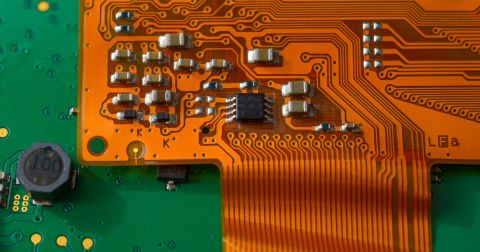
Unsupported Flex Fingers
This termination option is highly customizable and is essentially extensions of the conductors that are not encapsulated by coverlay or base materials on three sides. This creates a “free-floating” conductor that is accessible from either side of the flex. These flex fingers can be custom built to meet specific requirements for pitch, length and location and provide a robust termination while still retaining flexibility during installation and use. This method allows an easy direct connection to PCBs or other components. These unsupported flex fingers can be straight, or they can be bent for SMT assembly.
While this termination method may only require the finger thickness to simply be an extension of the copper conductor, the finger area is more often designed to have thicker, more robust fingers that taper down to a thinner copper thickness in the flexing area.
![Flex Pcb Design, Desiging Flexible Circuits Expert [With Complete Design Guide]](https://www.venture-mfg.com/wp-content/uploads/2018/11/Figure-18-Sculpured-flex-PCB.jpg)
Unsupported conductor fingers on a flex PCB.
Typically, conductor thickness in the finger area is 0.010” with the non-finger areas pre-etched to a thinner copper weight. These fingers are then formed, typically with laser ablation removing materials on 3 sides of the finger area. This option has the benefit of being customizable to meet exact application requirements, but it should also be cautioned that the extra processing for this option will increase cost. As a final note, this solution is prone to damage of the finger area prior to assembly. To mitigate this risk, it is common to minimize damage to the unsupported finger area by connecting all fingers with a bus bar holding all fingers in alignment.
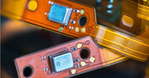
Crimped Contacts and Displacement Connectors
A third option is to mechanically crimp pins at each conductor. This method ensures a robust mechanical and electrical connection by piercing the circuit and wrapping the contact around each conductor. This method is available in both male and female mating options and typically in two standard pitches which meet most market needs. Centerline housings are also available to encapsulate the contact. This option is not as customizable as the unsupported finger termination method, but this is a lower cost option that also provides a robust connection alternative.

These crimp connector systems can mount onto a flex PCB. They give access to wiring or custom harnesses.
To answer the original question, nearly any connector option can be used in flexible circuit designs. But there are three common termination methods that are unique to flex; ZIF connectors, unsupported flex fingers and crimped contacts and displacement connectors. Each of these options has benefits, drawbacks and specific design criteria to be aware of.
PCB routing is much easier when you use the complete set of PCB layout tools in Altium Designer®. The integrated design rules engine ensures you can comply with all the important flex and rigid-flex DFM rules and component placement requirements. Every Altium Designer user also has access to a dedicated workspace in Altium 365™, where projects, component data, manufacturing data, and any other project documentation can be stored and shared with collaborators.
We have only scratched the surface of what’s possible with Altium Designer on Altium 365. Start your free trial of Altium Designer + Altium 365 today.
About Author
Related Resources
Related Technical Documentation
Table of Contents
Design to Release, Without the Friction
- Keep reviews tied to the right version
- Reduce handoff confusion and rework
- Spot sourcing and release risk earlier
- Work solo, share when needed
Get Started
Thank you, you are now subscribed to updates.