Mobile menu
PCB Design
Altium Designer
World’s Most Popular PCB Design Software
CircuitStudio
Entry Level, Professional PCB Design Tool
CircuitMaker
Free PCB design for makers, open source and non-profits
Why Switch to Altium
See why and how to switch to Altium from other PCB design tools
Solutions
For Enterprise
The Last Mile of Digital Transformation
For Parts and Data
Extensive, Easy-to-Use Search Engine for Electronic Parts
Altium 365
Resources & Support
Explore Products
Free Trials
Downloads
Extensions
Free Altium 365 Tools
Online PCB Viewer
Resources & Support
Renesas / Altium CEO Letter To Customers
All Resources
Support Center
Documentation
Webinars
Altium Community
Forum
Bug Crunch
Ideas
Training & Education
Professional Training / Certification
Comprehensive Career Training for Altium Software and Design Tools
University/Educators & Students
Academic Licenses, Training, Sponsorships and Certificates for Higher Education
Store
Search Open
Search
Search Close
Sign In
PCB Routing
Main menu
Home
PCB Design
Collaboration
Component Creation
Data Management
Design Outputs
ECAD/MCAD
HDI Design
High Speed Design
Multi-Board
PCB Layout
PCB Routing
PCB Supply Chain
Power Integrity
RF Design
Rigid Flex
Schematic Capture
Signal Integrity
Simulation
Software
Altium 365
Altium Designer
Enterprise Solutions
PDN Analyzer
Upverter
Education
Programs
Altium Academy
Engineering News
Guide Books
Newsletters
Podcasts
Projects
Training Courses
Webinars
Whitepapers
FREE TRIALS
Best in Class Interactive Routing
Reduce manual routing time for even the most complex projects.
Explore Solutions
PCB Routing
Overview
Webinars
A Brief Study of Stubs on a PCIe Connector
Stubs are an important topic in high-speed PCB design, and there is a longstanding guideline that stubs should always be
How to Start an FPGA PCB Layout For Your Embedded System
FPGAs are key elements that aid innovation in advanced embedded systems where ready-made SoCs may not be available. See why you should use an FPGA in your embedded system.
Addressing Skew Sources in High Speed PCBs
Sometimes, when we talk about skew, we aren't as specific as we should be. Most discussions of skew and jitter
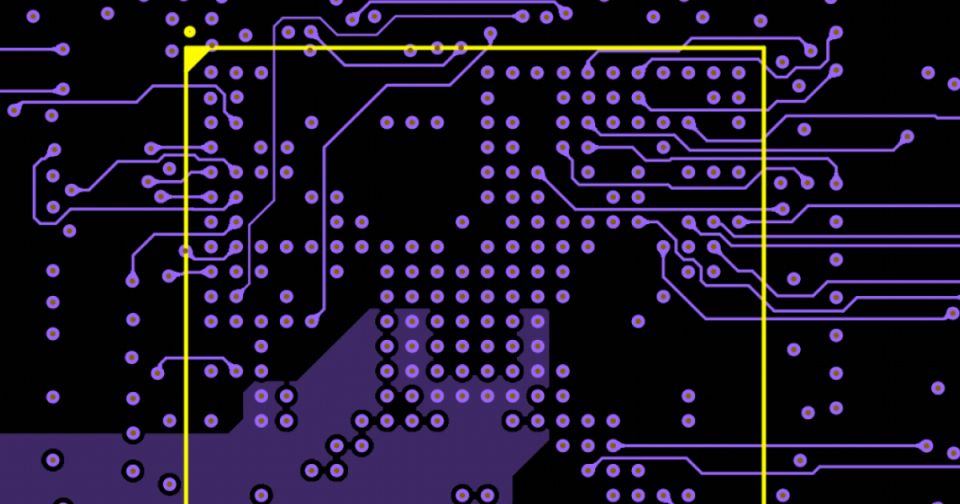
Pin-Package Delay and Via Delay in High Speed Length Tuning
Take a look at the inside of some integrated circuit packages, and you’ll find a number of wires bonded to
How to Successfully Design With a BGA
What's the first step in designing with a high pin count BGA in your PCB? You'll start with floorplanning, fanout, and layer assignment to aid routing.
OnTrack Podcasts
The Many Benefits of Additive Process in PCB Manufacturing
In this episode we will tackle the technology and the chemistry behind additive process in PCB manufacturing. Our guest Mike Vinson, Averatek’s COO will discuss the many benefits of this advanced PCB manufacturing process in designing sophisticated electronics.
Pagination
First page
« First
Previous page
‹‹
Page
9
Current page
10
Page
11
Page
12
Page
13
Page
14
Next page
››
Last page
Last »
💬
🙌
Need Help?
×
📞
1-800-544-4186
📞
1-858-864-1798
✉️
sales.na@altium.com
🛟
Support Center
📣
Ask Community
📞
Contact Us