Designing a 6-Layer PCB Stackup for Enhanced EMC

6-layer PCBs are an economical and popular stackup for a variety of applications with high net count and small size. Larger boards might work fine with a 4-layer stackup, where signal layers can be sacrificed to ensure isolation between each side of the board. With the right 6-layer stackup, you can suppress EMI between different layers and accommodate fine-pitch components with high net count. However, there are cases where it makes more sense to use a 4-layer or 8-layer stackup, and it helps to understand the function of plane layers in the board to make this judgement.
How Many Power, Ground, and Signal Planes Do I Need?
The answer to this question is extremely important and really depends on the application for your board. If you are routing a dense board with limited space, but everything is low speed or DC, you can often do just fine with two plane layers and four signal layers. However, in that case, you can often reduce the layer count to 4 layers with some creative layout and routing.
If you need to significantly reduce susceptibility to EMI, an alternative stackup is used, and you should opt for more power/ground and fewer signal layers. If this is a digital board or mixed signal board, the placement of signal with respect to plane layers, and a closely spaced power/ground plane pair, will give you the flexibility you need to route everywhere in the baord without creating an EMI problem. The addition of more ground around the board can also have a significant shielding effect without the need for an inelegant solution like shielding cans.
If you will be mixing digital and analog signals, mixing high and low frequency signals, or a combination of all of these, you can still make some creative use of a 6-layer PCB stackup. At some point, you might need to opt for a larger board or more layers in your stack (or both!). There are many signal/plane layer of combinations for 6-layer PCB stackups, but a few common ones will be shown below.
6-Layer PCB Stackup Examples
With this in mind, let’s dive into a few 6-layer PCB stackup examples:
Signal+PWR/GND/2 Signal Layers/GND/Signal+PWR
This 6-layer PCB stackup example is a popular entry-level option that provides shielding for low speed traces on the interior layer from traces on the outer layers. There is also tight coupling to solid planes. You can route signals with lower frequency/slower switching speeds or through an interior layer as long as they are orthogonal. I would route higher speed digital and/or analog signals on the outer layers in order to shield them from each other and the lower speed/frequency traces on the inner layers. An example is shown below.
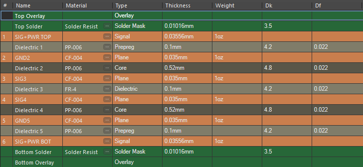
On this, I would not mix analog and digital in the inner layers unless you can separate them into different regions of the board. However, in that type of situation where you need separation between digital and analog sections, you can probably make due on a 4-layer stackup with internal planes and some creative layout/routing, or you can use the preferred SIG+PWR/GND/GND/SIG+PWR arrangement on 4 layers (see here for guidelines).
On this type of stackup, don't make layer 2 a power plane layer, and don't try to do broadside coupled pairs in parallel on L3+L4. Instead, you'll be routing PWR on a signal layer. The main problem with this is the lack of interplane capacitance between the power and ground plane layers and the high inductance return path from L1 to L5. Because these plane layers are separated, more decaps and ground return vias will be needed to compensate for the unpredictable return paths for signals on L1. For this reason, these boards should probably only be used with power or DC systems that do not need precise return path prediction and tracking.
Signal/GND/PWR/GND/Signal/GND
This 6-layer PCB stackup example is a good asymmetric stackup for boards that need to provide a lot of decoupling to high speed signals, but where the density isn't so high that you need 3 layers worth of signals. One example is a mix of high speed (L1) and low speed (l5) signals as these will be isolated from each other, and the closely spaced PWR+GND plane pair will provide high decoupling to support high speed power integrity. The interior signal layer will be shielded from the surface signal layer as it is encased between two ground planes. It is also useful for suppressing EMI from interfering with the interior signal layer as the solid conductors provide effective shielding. The power and ground planes will likely be closely spaced to provide effective decoupling for high speed digital devices.
The main problem with this stackup is that it only allows easy component placement on the top layer unless you start cutting out ground from the bottom layer to make room for components, so you're basically building only a 1-sided board. This is an expensive proposition for fab as it requires a lot of drilling to place vias to the internal signal layer. It highlights the advantages of a 4-layer or 8-layer PCB stackup. With an 8-layer stackup, you can create a similar arrangement of adjacent power/ground in the internal layers while also accommodating internal routing and components/routing on the bottom layer.
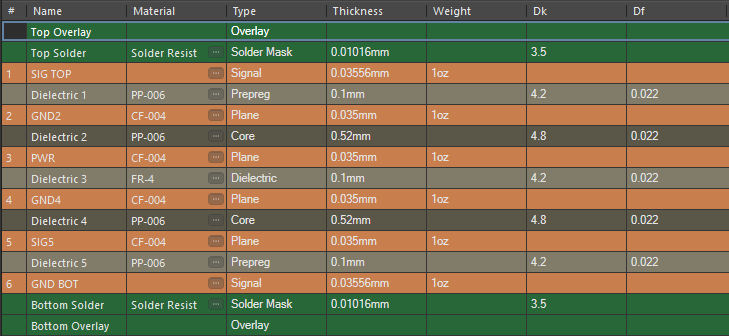
Signal/GND/PWR/Signal/GND/Signal
This is a variation on the previous board that provides an additional signal layer. This is a good starting point if you're working with a moderate I/O count digital system that requires impedance control on the outer layers. For example, we use this stackup on network switches and mixed signal boards running at Gbps or higher data rates. The drawback is the lower decoupling between PWR and GND compared to the previous stackup. The low PWR/GND coupling is compensated with banks of decaps. L4 can then be used with lower speed signals that are referenced to PWR, which will then have direct coupling back to GND on L2.

GND/Signal/PWR/GND/Signal/GND
If your board will be deployed in an electrically noisy environment, or if it will be placed near a source of strong radiation, this stackup provides excellent EMI suppression. With the addition of carefully spaced stitching vias, you can provide shielding up to some high frequency (usually well into the GHz range). The downside is that there are only two signal layers, so board space for routing signals will be limited. You will also be cutting up the PWR plane with vias when routing between the signal layers, or out to the surface layers. That being said, placing the signal layers between stacked conductive planes is a good choice from an EMC standpoint.
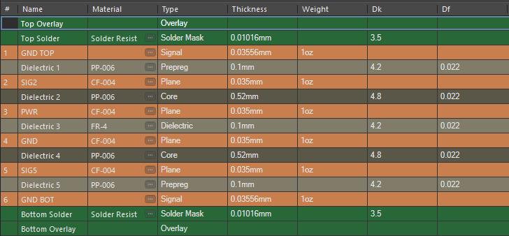
This layer stack provides another not-so-obvious benefit: better thermal management. Although these boards are not meant for power systems with high currents, the conductors on each side of a signal layer and in the internal layers can help transport heat to the board edges and surfaces, where it can then be dissipated with passive or active cooling. You won't have the same level of heat dissipation as you would with a metal-core board or a ceramic, but you've got the advantages of multiple planes for shielding to aid EMI suppression.
A Note on Routing Between Multiple Layers
We often talk about routing vias through multiple layers, but doing this can create a discontinuity in the return path that increases the loop area for the circuit. In this case, the parasitic capacitance between layers will have to provide some discharge that induces a return current near the signal via. Unfortunately, the capacitance is usually too small to provide a reliable low impedance return path. For this reason, the return path will appear in the nearest decoupling capacitor, or in the vias you use to connect the ground regions on multiple layers, all of which might be far from the signal via. The result is a very large return path with large loop inductance, and this will create a new EMC problem that you have to solve.
As a result, there are two common options that are cited as ways to eliminate the EMI from this lack of a return path:
- Place a decoupling capacitor in parallel with the signal via to provide the return path
- Place a grounded via or pair of grounded vias in parallel with the signal via to provide the return path
In my opinion, the better option is to place one or two a grounded via running alongside the signal via as long as the two reference planes are at the same potential. This provides a return path with low inductance and without breaking the coupling to the reference planes. This need to provide a return path is one reason a designer might just fill everywhere in the layout with grounded stitching vias once the layout is finished. If you do this with stitching vias, make sure to read this article.
To see some other use cases involving 6-layer stackups to provide EMI suppression, specifically in IoT products, take a look at Ken Wyatt's recent AltiumLive 2022 presentation.
Your PCB design package should include the tools you need to design your stackup entirely from scratch. With Altium , you’ll have full control over your layer arrangement, material constants, and dimensions. You’ll even be able to use the layer stack manager to create rigid-flex and multi-board systems with ease. All these design tools integrate directly with your schematic design, layout, and deliverable generation tools in a single program.
Download a free trial of Altium to see how the powerful tools give you full control over your board. You’ll also have access to 6-layer PCB stackup examples and the best design features the industry demands in a single program. Talk to an Altium expert today to learn more.
Trade In Your Outdated PCB Design Tool & Unlock 45% OFF Altium today!

About Author
Related Resources


Related Technical Documentation


Table of Contents
Take advantage of the world's
most trusted PCB design system.
One interface. One data
model. Endless possibilities.
Effortlessly collaborate with
mechanical designers.
The world's most trusted
PCB design platform
Best in class interactive
routing
View License Options
Thank you, you are now subscribed to updates.