Component Warpage Causes in a PCB
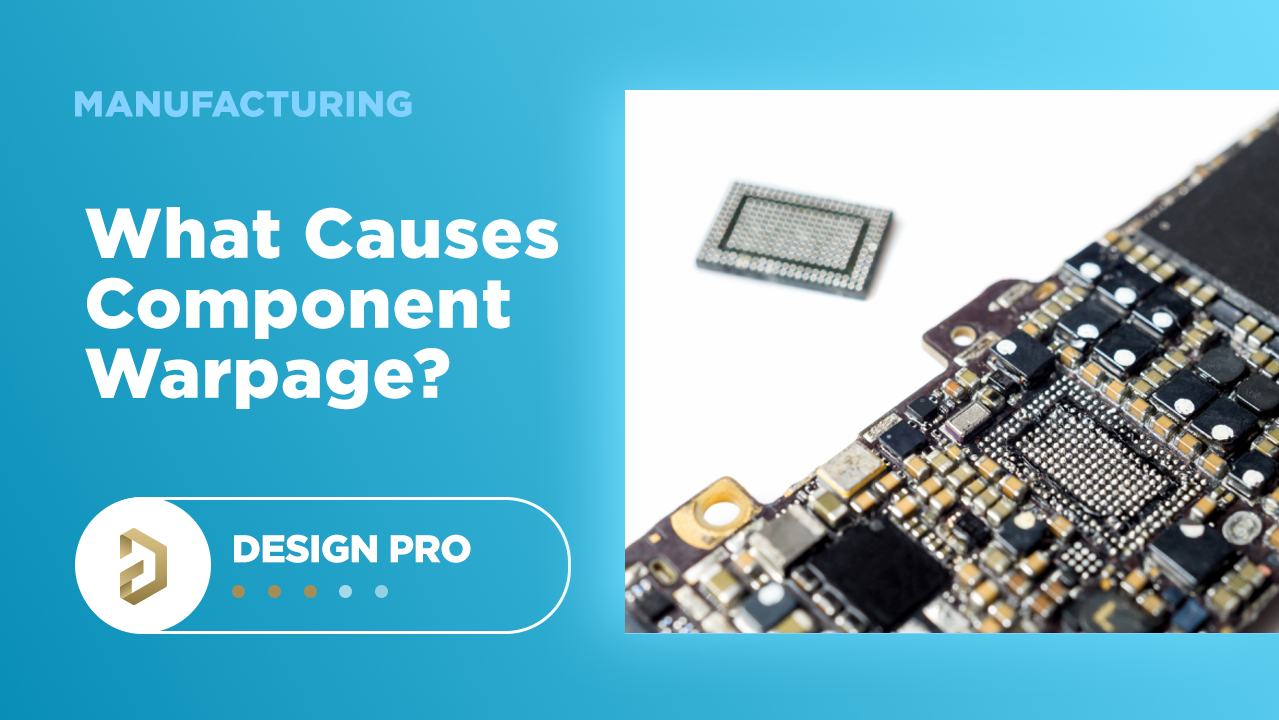
A staff member at a PCB manufacturer once explained to me that they thought we were having an issue with a package warping. Prior to this I had assumed that this was highly unlikely in standard component packages used in a PCBA. Unfortunately, component warping can occur both in a PCB and in components. Mechanical mishandling leading to bending is an obvious one, but there are potentially other problems that could cause component warpage without a mechanical impact being involved.
In this article, we'll give an overview of warpage in a PCB, specifically in the circuit board and in the components. The possibility of warpage in the circuit board should be obvious given that PCB laminate materials are slightly flexible, but the potential for warping in components is not so obvious.
Where PCB Component Warpage Occurs
Component warpage can occur during PCB assembly, or your components could have been warped before arriving at the assembly facility. Occasionally, you’ll receive components with warped packaging, either bent or otherwise not perfectly flat, which occured during manufacturing or shipping. Most of the time, warping is very slight in most components and assemblies, and the presence of such warpage will cause no problems in the functionality or reliability of the assembly.
When warping is more severe, it may be difficult to find anything wrong before you start testing components or using the device. Unfortunately, once components arrive at an assembly facility you are probably in no position to start testing them in a fixture or inspecting them for flatness. Unless they are very obviously warped, they will be put into pick-and-place straight away. After you’ve incorporated those components onto your board, you’ll be hard pressed to prove whether the warping occurred before or after your processing and handling.
To brielfy sum up, warpage can arise in the following situations:
- During component production, where components were not properly screened during production or packaging
- During PCB assembly, where the soldering process creates a defect in the component
- When the PCB warps, which can then force warpage to occur in some components
- During transport, where some mechanical impact or shock damages the board and/or components
Assembly Defects That Cause Component Warpage
The impact of component warping may be small enough that you’ll never notice, or it might cause latent electrical issues. Arguably the worst case is when repeated cycling and warpage weakens a solder joint enough to cause a premature or intermittent failure. The factors that can lead to warpage in components during assembly include:
- Thermal cycling
- CTE mismatch
- Outgassing
The simplest case where repeated cycling causes component warpage is due to repeated cycling. One are where these electrical issues will show up is in large processors with ball grid array packages, where components have a large surface area to be affected by warping. Packages on an organic substrate can also be affected by thermal cycling and experience warpage as they can have a CTE mismatch compared with surrounding laminates.
When the mismatch between a component package and the board is large, warpage will set in and increase the distance between the PCB and casing, and there are a couple possible outcomes. In some cases, if a solder ball “drops” and stays low to the PCB rather than connecting to the component, an open circuit could result or the solder could flow and bridge other connections. Otherwise, the solder ball will stretch to make the connection at the appropriate temperature. You see a circuit, but the solder in the join is thinned, and sometimes weirdly shaped, making the joint will be less reliable over time. The impacts are much worse as the pitch between BGA pads decreases.
If the surface warps down, usually with corners and edges slumping during reflow, then you’ll suddenly have too much solder under your component. It will often squish off of the pad, bridging to other solder pads and shorting them together, like you see in the image below.
It’s even possible, though rare, to have poor manufacturing result in outgassing. This can create a bubble inside packaging or force a casing askew. However, the most common cause is thermal issues. Rework may cause warping in your components during reflow processing, or a thermal mismatch between the packaging and solder can cause warping when materials experience thermal expansion at different rates.
To learn more about circuit board warpage and some strategies for preventing PCB warpage, take a look at this article.
Some Simple Practices For Preventing Warpage
Fortunately, there are a few options that can help prevent or reduce warping. First, use solder mask defined pads because non-solder mask defined pads will have much lower molten solder height. That’s because molten solder doesn’t have as much wicking area to spread out over. You can also adjust the process materials and temperatures, often bringing temperatures down, or reducing the thermal mismatch between a leadless solder and components can dramatically improve your outcomes. If you have corners slumping during reflow, you can use spacers to support them until they’ve cooled.
Finally, limit the number of solder/rework cycles, and do not fixate the PCB during soldering cycles. The thermal stress induced in the PCB can lead to warping in the components, in the PCB, or both. Primarily this is a PCB challenge, but repeated thermal cycling in board regions with high mismatch can lead to component warpage, particularly in packages with an organic substrate and in BGAs. An understanding of the components in your board can help you identify which parts will have lower changes of assembly defects during production or rework.
When you need to specify your design and production requirements and prepare your board for manufacturing, use the complete set of PCB design tools in Altium Designer®. When you’ve finished your design, and you want to release files to your manufacturer, the Altium 365™ platform makes it easy to collaborate and share your projects.
We have only scratched the surface of what’s possible with Altium Designer on Altium 365. Start your free trial of Altium Designer + Altium 365 today.

