
Need a 4-layer PCB stackup that can support high speed components on both sides of the board? Consider these alternatives to the typical 4-layer stackup.
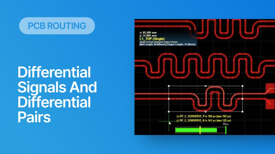
Differential pairs and differential signaling are the mainstay of high speed digital communication and data transfer.
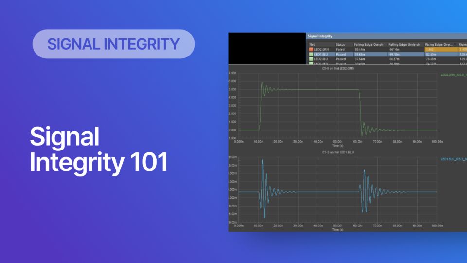
Learn about the basics of signal integrity and how you can ensure your PCB layout complies with best practices for signal integrity.
Circuit protection from transient voltages and currents can be applied with ESD protection circuit designs. Learn more about these circuits in our guide for new engineers.
Use the best circuit schematic editor to create your next electronic design and start your PCB layout.
Want to know about multi-PCB design? Learn more about what is multi-board design and how to use native 3D design with ECAD MCAD collaboration aids complex PCB layout.
You can use the DNI/DNP designation on components in your PCB BOM to create design variants as long as you’ve created your layout correctly.