Which Type of Opto-Isolator Is Right For Your Circuit?
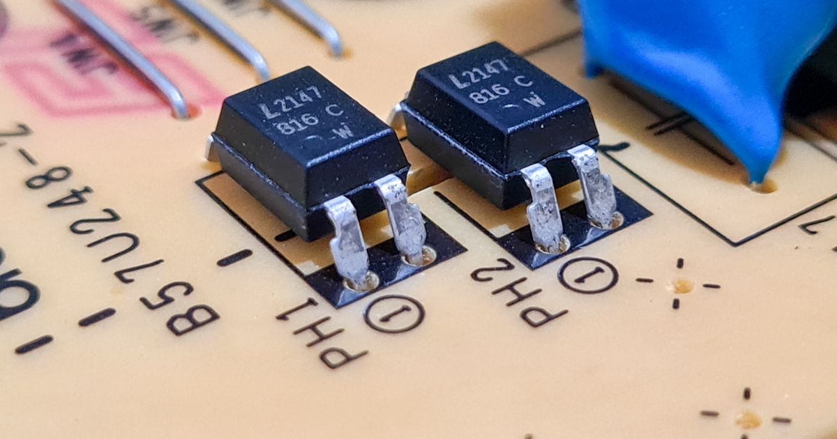
An optoisolator is an electronic device that can be used to pass information between a diode without passing an electrical current. Because there is no need to directly pass voltage or current between the inputs and outputs in an optoisolator circuit, these components can be used to provide electrical isolation in two regions in a PCB. Opto-isolators act as a protection mechanism, ensuring that harmful electrical currents cannot flow across the device, protecting the system from high voltages.
In simplest terms, an optoisolator works by taking an input electrical signal and converting it into a light signal using a light-emitting diode, generally operating in the near-infrared spectrum. Then, within the same device, a light-sensitive device such as a photodiode, phototransistor, or photodarlington transistor converts the light signal back into an electrical signal. This provides a barrier to any voltage transients or overvoltage levels that appear at the input from affecting the electrical circuit at the output of the optoisolator. The components are sealed in an opaque package to prevent interference from external light.
Many different types of optoisolator circuits are widely used in communications, control, and monitoring systems where data signals could provide a point of ingress for harmful voltages to damage a device. They are particularly useful where long data cables that could be susceptible to induced voltage transients or ground plane surges enter an electronic device containing sensitive semiconductor components.
Important Specifications in Optical Isolation
It’s worth mentioning that the terms optocouplers and optoisolators are often used interchangeably; however, the usual convention is that optocouplers are devices that can isolate voltages of up to about 5000V while optoisolators are devices that can isolate voltages of over 5000V. Don’t be surprised if you see exceptions to this convention. There are also different optoisolator speeds, and fast optoisolators like a solid state relay will outperform something like a diode optoisolator in terms of data transfer. If in doubt, study the data sheet. The image below shows the typical circuit diagram for an optoisolator with inputs on the left and outputs on the right. This is also the symbol for octocouplers.

For the moment, we want to focus on the different types of optoisolators. When choosing an optoisolator, the key parameters to consider are the isolation voltage, bandwidth, linearity, current transfer ratio, and power requirements.
Optical Isolation Voltage
The isolation voltage is the maximum rated voltage difference that can be present between the LED and the light sensor. This isolation voltage is governed by the construction of the optoisolator device itself and factors outside the device. An internal breakdown will occur when the voltage at the light source element of the device arcs across to the light sensor element. Similarly, an external breakdown will occur when the voltage at the input pin of the device arcs across to an output pin. This is affected by the PCB design, which is how the traces for the inputs and outputs are routed and separated and the environmental conditions around the device. The voltage at which arcing will occur will depend on the temperature, humidity, separation distance, pressure, and airborne contaminants’ presence. Distance and humidity are the most significant factors. Typical off-the-shelf optoisolators can withstand input-to-output voltage differences of up to 10 kV and voltage transients of around 25 kV/μs.
Bandwidth
Where an optoisolator circuit is used to decouple ground planes or voltage sensing inputs, the rate of change of the isolated signal is relatively unimportant. However, where the optoisolator is used to decouple data links and communications lines, the device’s throughput becomes essential. Typical applications range from relatively slow-speed serial data links such as I2C or SPI running at tens of Mbps to high-speed protocols running at Gbps. The more basic optoisolators typically have a bandwidth of around 10 MHz (See below), but there are devices specifically designed for faster data rates. Bear in mind that the achievable data rate for any optoisolator circuit will depend on how the output is loaded and affected by temperature. Study the datasheet very carefully if you’re isolating fast data links.

It is worth mentioning that off-the-shelf passive network isolators are available for wired Ethernet networks that use electromagnetic induction to provide an electrically non-conducting barrier without the requirement for an external power supply. Implementing an optoisolator circuit may not always be the most appropriate solution, but that decision will depend on your individual circumstances.
Linearity
As with any semiconductor device, the photodiode used in the optoisolator will have an element of non-linearity in the relationship between the input and output, which can distort the signal being passed through the isolator. Ensuring the photodiode is biased and operated in its linear range, avoiding the cutoff or saturation regions, will reduce this effect to some extent. Any residual non-linearity will be particularly noticeable where the optoisolators are used to decouple analog signals.
Specialist analog optoisolators have been developed with minimal non-linearity. Typically, they use two photodiodes connected to an operational amplifier. One photodiode operates as usual, while the second device with identical non-linearity performance sits in the amplifier’s feedback loop to compensate by canceling out the non-linearities.
Current Transfer Ratio
The current transfer ratio (CTR) is the ratio between the LED and sensor currents, effectively gaining the device and reflecting its efficiency. Opto-isolators with a low CTR will require more current to drive the LED to create sufficient current at the phototransistor for a particular output load.
The CTR is not constant but is dependent on the input current coming into the component. The CTR will also vary with each component, its temperature, and the component’s age, so it’s crucial to select a device that delivers the required CTR at the maximum rated temperature and maximum operating life of the device the optoisolator will be using. Manufacturing tolerances in components can lead to wide ranges of CTR within the same batch of components, so the design must work based on the minimum CTR stated in the data sheet. All these factors can make the selection of the optimum device tricky. If in doubt, add a healthy margin for error and simulate the optoisolator circuit using worst-case component values to ensure the circuit will work correctly.
Power
The final factor to bear in mind is the power requirements of the optoisolator circuit itself and the management of heat generated by the component due to losses. Basic components can be relatively inefficient and generate significant thermal energy levels that must be appropriately handled, particularly as the performance of the optoisolator itself will be adversely affected by heating effects. When designing the circuit layout, remember to keep the input traces to the optoisolator circuit suitably separated from all other traces, especially ground and power planes, to prevent transients from being capacitively or inductively coupled between traces.
Opto-isolators Construction
Opto-isolators typically use a near-infrared LED to convert an electrical input signal into an equivalent light signal. The light is contained within a closed optical isolation channel, also referred to as a dielectric channel. A photo-sensing device at the end of the optical isolation channel either directly generates an electrical signal from the received light or uses the received light to modulate the electric current that flows from an external power source. The photo-sensing device can be a photoresistor, photodiode, phototransistor, silicon-controlled rectifier (SCR), or triac. As photoresistors can be used both as a light source and a photo-sensing device, it is possible to form a bidirectional optoisolator using two photoresistors, one at each end of the optical isolation channel. Performance and efficiency issues limit the availability and application of bidirectional optoisolators. An equivalent circuit can be implemented using two unidirectional optoisolators in a reversed configuration at the expense of requiring more discrete components with a much greater footprint.

The physical layout of optoisolators depends primarily on the desired isolation voltage. Devices rated for less than a few kV typically have planar construction. The sensor die is covered with a sheet of glass or clear plastic, which is topped with the LED die. The absorption spectrum of the sensor will be matched to the output spectrum of the LED. The thickness of the optical isolation channel determines the rated breakdown voltage of the device. Devices rated for higher breakdown voltages typically have silicone dome construction. The LED and sensor die are placed on the opposite side of the package, separated by a gap formed by a transparent silicone dome. The dome is shaped to direct the maximum amount of light possible from the LED to the sensor.
Application
Electronic equipment and signal and power transmission lines can be regularly subjected to voltage surges induced by lightning and electrostatic discharge, radio frequency interference, and pulses generated by load changes. As discussed in a previous article, remote lightning strikes can induce several kV surges into long communications and power lines. Opto-isolators can provide a solution to preventing voltage surges present at the inputs to a device from affecting the more sensitive components within that device. There are also applications where a device incorporates elements that employ high voltages as part of the design. The design may well require an interface between the circuit’s high-voltage elements and the standard low-voltage elements. Opto-isolators can also help keep the different elements safely separate in this instance.
Where optoisolators are used to drive digital logic levels, the output configuration needs to be taken into account. If the output of the optoisolator is required to swing from zero volts to the power rail to accommodate the load circuit, an optoisolator with a Totem-Pole output configuration will be required. Otherwise, the more common Push-Pull configuration can be chosen.
The main feature of optoisolators that differentiates them from equivalent isolating transformers is no energy flows across the device. They operate by modulating electrical energy supplied to the output to reflect the level of energy reaching the input. However, one significant advantage that optoisolators have over isolating transformers is that they can transfer very low-frequency signals all the way down to DC levels. They are also simpler to implement into an optoisolator circuit design as the input and output impedances are independent, requiring no additional components for impedance matching.
Types of Sensors in Opto-isolators
Photoresistors
Photoresistors are non-polar devices used in both DC and AC circuits. They operate by changing their resistance in reverse proportion to the intensity of the received light energy. The operating range of the resistance can be from a few hundred Ohms up to an open circuit. Traditionally used in telephony and industrial automation, they have been superseded in the main apart from niche applications in musical instrument amplification.
Photodiodes
When light energy falls on a photodiode, a charge is generated proportional to the intensity of the received light energy. This small charge can be used to drive a high impedance load, and the photodiode is operating in a photovoltaic mode. When a photodiode is reverse-biased using an external voltage source, received light energy will increase the reverse current flowing through the diode, modulating the flow of energy from the external source. The energy flow rate is directly proportional to the received light energy intensity when operating in this photoconductive mode. By incorporating LED drivers and output amplifiers into the optoisolator's device, the photodiode operating in this photoconductive mode can be optimized to operate at relatively high speeds. This is the type of sensor you will find in a high-functioning, fast optoisolator circuit.
Phototransistors
Phototransistors are inherently slower than photodiodes and must be correctly biased and loaded to achieve speeds in the tens of kHz. However, their open collector output means that they have the advantage of being able to generate larger output currents and are more sensitive. They are more suited for use in DC circuits where the slower response time will have no impact. Using a Schottky clamp on the phototransistor’s open collector output can provide relatively good linearity in the device’s response.
The photodarlington is a variant of a phototransistor where a pair of transistors in the Darlington Pair configuration provides much higher levels of gain and sensitivity than a standard phototransistor at the cost of a slower response rate.
Photo-Silicon-Controlled rectifiers
Silicon-controlled rectifier (SCR) optoisolators are a type of thyristor-based isolator designed for AC power control applications. Also known as photo-SCRs, they provide complete isolation of noise and voltage transients present on the AC power supply line. Performance limitations from only operating across the positive half of the main AC cycle make their use less common than photo-triac devices.
Photo-Triac
Photo-triac (triode for alternating current) optoisolators are, like photo-SCRs, optimized for use in solid-state relay applications to control AC’s mains-powered loads. The triac optoisolator can safely operate a high-voltage AC supply from a simple switched DC input. Unlike photo-SCRs, a triac optoisolator can operate across the entire mains AC cycle with zero-crossing detection allowing the circuit to drive full power to the load with minimal inrush current when switching inductive loads.
Photo-MOSFET
Photo-MOSFET (metal–oxide–semiconductor field-effect transistor) relays are a less common type of optoisolator designed for fast-switching applications where high reliability and long life are required in environmentally challenging conditions. Capable of efficiently switching 1.5 kV and handling currents of up to 5 A with no contact bounce, these solid-state devices are utilized in the latest generation of battery management systems for solar power generation plants and electric vehicles.
Conclusion
When choosing between types of optoisolators, don’t just go for whatever device fits your budget and is in stock at your favorite supplier. Opto-isolators come in a broad range of different types that are optimized for particular applications. Start the selection process by considering the key factors;
- What is the highest voltage you need to protect against?
- Do you require a faster data-transfer rate provided by a fast optoisolator circuit?
- What is the bandwidth of the signal that you are looking to isolate?
- Do you need to isolate DC or AC, or are you looking at isolating a high-speed data line?
- How are you powering the output, and what load is it driving?
- Knowing this and the characteristics of the input, what is the current transfer ratio you’ll need?
- Then, how will you incorporate the optoisolator (s) into your design, and what thermal management measures will you need to include?
The lesson here is that merely dropping in an optoisolator circuit device onto your board is not as straightforward as it may first appear. It must be considered part of the overall design process from day one to guarantee your circuit works correctly. Opto-isolators are great for decoupling DC and low-frequency signals from the rest of the circuit, but they require external power, and they generally have a poor high-frequency response. Transformer isolators are excellent at high frequencies but can’t handle DC signals. However, the calculations for handling the inductance that adds to the circuit and the requirement for impedance matching can make them unsuitable for some applications. Another consideration is that the optoisolator chip will be significantly smaller than an equivalent transformer isolator and far simpler to fit onto a circuit board. And finally, don’t forget the power of simulation tools to help ensure you make the right choices.


