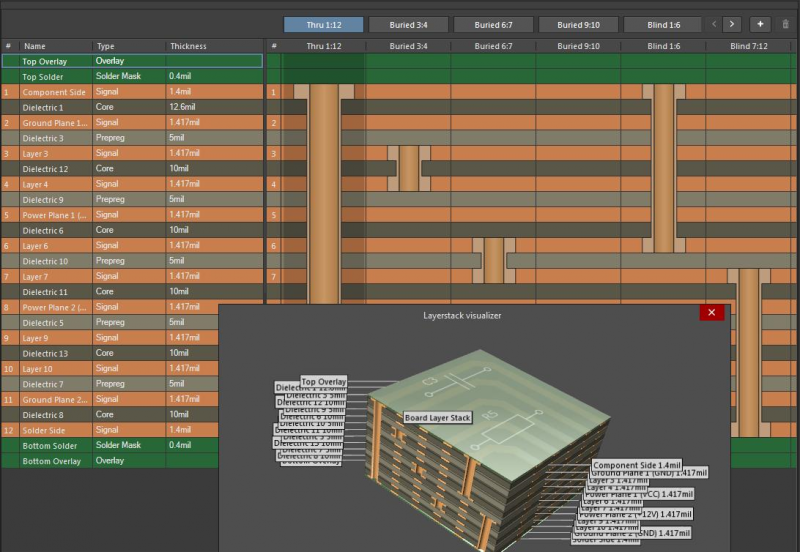
Multi-Layer PCBs & Layer Stackup
Browse our library of resources to learn more about multi-layer PCB design & layer stackup.
가이드북
Explore Guidebooks for Multi-Layer PCBs and PCB Layer Stackup and start creating today!


Videos
Watch videos for Multi-Layer PCBs and PCB Layer Stackup to learn more!


Technical Documentation
Explore Technical Documentation related to Multi-Layer PCBs & Layer Stackup

Articles
Explore more popular content for Multi-Layer PCBs and PCB Layer Stackup!