Skip to main content
Mobile menu
Discover
Develop
Agile
Resources & Support
Free Altium 365 Tools
Gerber Compare
Online PCB Viewer
Resources & Support
Learning Hub
Support Center
Documentation
Webinars
Altium Community
Forum
Bug Crunch
Ideas
Education
Student Lab
Educator Center
Altium Education Curriculum
Search Open
Search
Search Close
Sign In
Main menu
Home
PCB Design
Collaboration
Component Creation
Data Management
Design Outputs
ECAD/MCAD
HDI Design
High Speed Design
Multi-Board
PCB Layout
PCB Routing
PCB Supply Chain
Power Integrity
RF Design
Rigid Flex
Schematic Capture
Signal Integrity
Simulation
Software
Develop
Discover
Agile
Altium 365
Altium Designer
Education
Programs
Altium Academy
Engineering News
Guide Books
Newsletters
Podcasts
Projects
Training Courses
Webinars
Whitepapers
Round and Curved PCB Design in Altium Designer
Our modern lives would not be possible without electronics. Sometimes it seems like a race to be the first person to wire everything in your house onto PCBs. With the multitude of possible device shapes and sizes, circular or rounded PCBs are becoming more popular. If you want to design your next device on a round PCB, your design software needs CAD and layout tools that don’t constrain you to working on rectangular PCBs. When you work with
Read Article
Customizing AI for Your Application
AI technology is quickly changing how devices interact with the world. Traditionally, a programmer has to predetermine how a system will react to the various and unpredictable circumstances that can arise in real-world scenarios. With AI, a model can be trained that captures desired reactions in such a way that the model can reliably provide desired reactions to circumstances that were never anticipated. One challenge for developers new to AI is
Read Article
Bringing AI to Market the Easy Way
There are numerous resources available that can enable you to bring AI into your product line. However, if you are new to AI, the path from prototype to production can seem daunting. There are new technologies to consider, making developing an AI model a very different beast compared to traditional linear programming. Estimating the processing and memory resources you’ll need can seem somewhat challenging as well. While implementing AI can be
Read Article
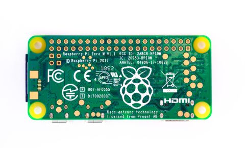
Production-Grade Battery Modules for Raspberry Pi Zero
I’ll admit, I’m a big fan of Raspberry Pi. This set of inexpensive boards packs plenty of general purpose computing power into a small form factor, it easily connects to a LAN/WiFi and is accessible via SSH, and its memory is easily expandable with a micro SD card. It’s also easy to get a new prototype embedded application up and running directly from your laptop. The one aspect that prevents its application as a production-grade embedded system
Read Article
PCB Design Review and Collaboration in Altium 365
Remote collaboration tools are everywhere these days, and now designers have access to a convenient collaboration system for electronics design. Whether you’re part of a design team, or you need to quickly execute any design changes recommended by your manufacturer, you need cloud collaboration tools that are immediately accessible within your PCB design application. Now with Altium 365, you’ll have access to a cloud-driven design interface that
Read Article
Differential Pair Length Matching: Best Practices for Signal Integrity
Length tuning/delay tuning is one important aspect of high speed routing with differential pairs. Read on to learn all about Altium's differential pair length tuning capabilities.
Read Article
How Do Pads and Vias Impact Total Capacitor Parasitic Inductance?
In this blog article we discuss how the footprint and mounting style affect capacitor parasitic inductance. The pads and vias back to the PCB power planes increase the total series inductance of the capacitor.
Read Article
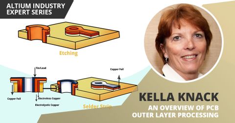
An Overview Of PCB Outer Layer Processing
Expert Kella Knack describes in detail the fabrication of the PCB outer layer. Read and learn about how different vias are formed and the steps involved in the multilayer build-up process.
Read Article
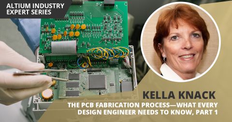
The PCB Fabrication Process—What Every Design Engineer Needs To Know, Part 1
In the olden and not-so-olden days of PCB development, the process of moving a board from design to manufacturing was often referred to as “throwing the design over the wall.” This was not the result of the operations being so clearly divided, but rather a way to assign ownership and blame if there were errors. My last project at Martin Marietta was a black hole program for the U.S. Airforce and Navy. When problems were encountered during the
Read Article
Working with Design Variants
Introduction They say variety is the spice of life. That is also the case for PCB designs. It may come as a shock to some, but many companies are in business and always chasing this thing called “profits” (I am using my sarcastic voice). It is entirely understandable that profit is what keeps the doors open and people employed. A significant way that they improve the bottom line is to have a variety of product lines available to their customers
Read Article
Pagination
First page
« First
Previous page
‹ Previous
…
Page
184
Page
185
Page
186
Page
187
Current page
188
Page
189
Page
190
Page
191
Page
192
…
Page
200
Page
210
Page
220
Page
230
Page
240
Page
250
Page
260
Page
270
Page
280
Page
290
Page
390
Next page
Next ›
Last page
Last »
Subscribe to